AD7785
Rev. 0 | Page 15 of 32
STATUS REGISTER
RS2, RS1, RS0 = 0, 0, 0; Power-On/Reset = 0x88
The status register is an 8-bit read-only register. To access the ADC status register, the user must write to the communications register,
select the next operation to be a read, and load Bit RS2, Bit RS1, and Bit RS0 with 0.
Tabl e 11 outlines the bit designations for the status
register. SR0 through SR7 indicate the bit locations, and SR denotes that the bits are in the status register. SR7 denotes the first bit of the
data stream. The number in parentheses indicates the power-on/reset default status of that bit.
SR7 SR6 SR5 SR4 SR3 SR2 SR1 SR0
RDY(1)
ERR(0) 0(0) 0(0) 1 (1) CH2(0) CH1(0) CH0(0)
Table 11. Status Register Bit Designations
Bit Location Bit Name Description
SR7
RDY Ready Bit for ADC. Cleared when data is written to the ADC data register. The RDY bit is set automatically
after the ADC data register has been read or a period before the data register is updated with a new
conversion result to indicate to the user not to read the conversion data. It is also set when the part is
placed in power-down mode. The end of a conversion is indicated by the DOUT/
RDY pin also. This pin can
be used as an alternative to the status register for monitoring the ADC for conversion data.
SR6 ERR
ADC Error Bit. This bit is written to at the same time as the
RDY bit. Set to indicate that the result written to
the ADC data register has been clamped to all 0s or all 1s. Error sources include overrange and underrange.
Cleared by a write operation to start a conversion.
SR5 to SR4 0 These bits are automatically cleared.
SR3 1 This bit is automatically set on the AD7785.
SR2 to SR0 CH2 to CH0 These bits indicate which channel is being converted by the ADC.
MODE REGISTER
RS2, RS1, RS0 = 0, 0, 1; Power-On/Reset = 0x000A
The mode register is a 16-bit register from which data can be read or to which data can be written. This register is used to select the
operating mode, update rate, and clock source.
Tabl e 12 outlines the bit designations for the mode register. MR0 through MR15 indicate
the bit locations, MR denoting the bits are in the mode register. MR15 denotes the first bit of the data stream. The number in parentheses
indicates the power-on/reset default status of that bit. Any write to the setup register resets the modulator and filter and sets the
RDY
bit.
MR15 MR14 MR13 MR12 MR11 MR10 MR9 MR8
MD2(0) MD1(0) MD0(0) 0(0) 0(0) 0(0) 0(0) 0(0)
MR7 MR6 MR5 MR4 MR3 MR2 MR1 MR0
CLK1(0) CLK0(0) 0(0) 0(0) FS3(1) FS2(0) FS1(1) FS0(0)
Table 12. Mode Register Bit Designations
Bit Location Bit Name Description
MR15 to MR13 MD2 to MD0 Mode Select Bits. These bits select the operational mode of the AD7785 (see Table 13).
MR12 to MR8 0 These bits must be programmed with a Logic 0 for correct operation.
MR7 to MR6 CLK1 to CLK0
These bits are used to select the clock source for the AD7785. Either an on-chip 64 kHz clock or an external
clock can be used. The ability to override using an external clock allows several AD7785 devices to be
synchronized. In addition, 50 Hz/60 Hz is improved when an accurate external clock drives the AD7785.
CLK1 CLK0 ADC Clock Source
0 0 Internal 64 kHz Clock. Internal clock is not available at the CLK pin.
0 1 Internal 64 kHz Clock. This clock is made available at the CLK pin.
1 0
External 64 kHz Clock Used. An external clock gives better 50 Hz/60 Hz rejection. See
specifications for external clock.
1 1 External Clock Used. The external clock is divided by 2 within the AD7785.
MR5 to MR4 0 These bits must be programmed with a Logic 0 for correct operation.
MR3 to MR0 FS3 to FS0 Filter Update Rate Select Bits (see Table 14).
AD7785
Rev. 0 | Page 16 of 32
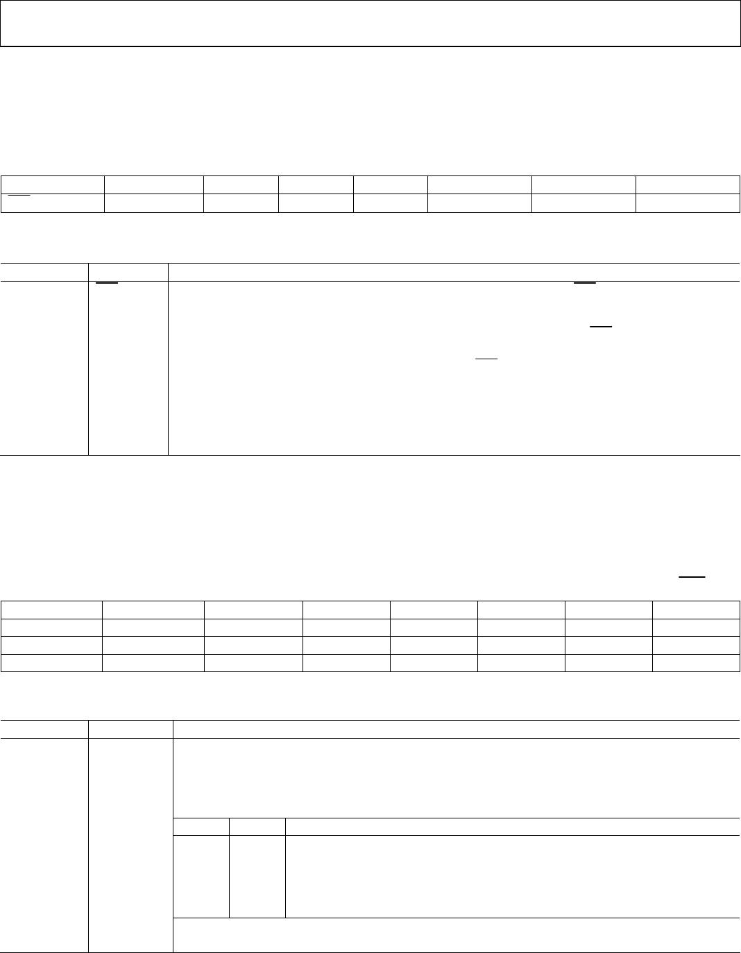
Table 13. Operating Modes
MD2 MD1 MD0 Mode
0 0 0
Continuous Conversion Mode (Default).
In continuous conversion mode, the ADC continuously performs conversions and places the result in the data
register.
RDY goes low when a conversion is complete. The user can read these conversions by placing the device in
continuous read mode, whereby the conversions are automatically placed on the DOUT line when SCLK pulses are
applied. Alternatively, the user can instruct the ADC to output the conversion by writing to the communications
register. After power-on, a channel change, or a write to the mode, configuration, or IO registers, the first conversion
is available after a period of 2/f
ADC
. Subsequent conversions are available at a frequency of f
ADC
.
0 0 1
Single Conversion Mode.
When single conversion mode is selected, the ADC powers up and performs a single conversion. The oscillator
requires 1 ms to power up and settle. The ADC then performs the conversion, which takes a time of 2/f
ADC
. The
conversion result is placed in the data register,
RDY goes low, and the ADC returns to power-down mode. The
conversion remains in the data register, and
RDY remains active low until the data is read or another conversion is
performed.
0 1 0
Idle Mode.
In idle mode, the ADC filter and modulator are held in a reset state, although the modulator clocks are still provided.
0 1 1
Power-Down Mode.
In power-down mode, all the AD7785 circuitry is powered down, including the current sources, burnout currents,
bias voltage generator, and CLKOUT circuitry.
1 0 0
Internal Zero-Scale Calibration.
An internal short is automatically connected to the enabled channel. A calibration takes 2 conversion cycles to
complete.
RDY goes high when the calibration is initiated and returns low when the calibration is complete. The
ADC is placed in idle mode following a calibration. The measured offset coefficient is placed in the offset register of
the selected channel.
1 0 1
Internal Full-Scale Calibration.
A full-scale input voltage is automatically connected to the selected analog input for this calibration.
When the gain equals 1, a calibration takes 2 conversion cycles to complete. For higher gains, 4 conversion cycles
are required to perform the full-scale calibration.
RDY goes high when the calibration is initiated and returns low when the calibration is complete. The ADC is placed
in idle mode following a calibration. The measured full-scale coefficient is placed in the full-scale register of the
selected channel.
Internal full-scale calibrations cannot be performed when the gain equals 128. With this gain setting, a system full-
scale calibration can be performed.
A full-scale calibration is required each time the gain of a channel is changed to minimize the full-scale error.
1 1 0
System Zero-Scale Calibration.
The user should connect the system zero-scale input to the channel input pins as selected by the CH2 to CH0 bits. A
system offset calibration takes 2 conversion cycles to complete.
RDY goes high when the calibration is initiated and
returns low when the calibration is complete. The ADC is placed in idle mode following a calibration. The measured
offset coefficient is placed in the offset register of the selected channel.
1 1 1
System Full-Scale Calibration.
The user should connect the system full-scale input to the channel input pins as selected by the CH2 to CH0 bits.
A calibration takes 2 conversion cycles to complete.
RDY goes high when the calibration is initiated and returns low
when the calibration is complete. The ADC is placed in idle mode following a calibration. The measured full-scale
coefficient is placed in the full-scale register of the selected channel.
A full-scale calibration is required each time the gain of a channel is changed.
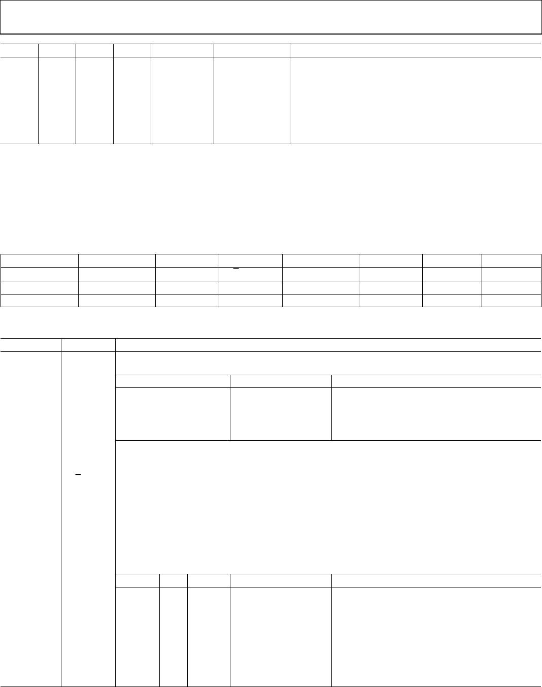
Table 14. Update Rates Available
FS3 FS2 FS1 FS0 f
ADC
(Hz) t
SETTLE
(ms) Rejection @ 50 Hz/60 Hz (Internal Clock)
0 0 0 0 x x
0 0 0 1 470 4
0 0 1 0 242 8
0 0 1 1 123 16
0 1 0 0 62 32
0 1 0 1 50 40
0 1 1 0 39 48
0 1 1 1 33.2 60
1 0 0 0 19.6 101 90 dB (60 Hz only)
AD7785
Rev. 0 | Page 17 of 32
FS3 FS2 FS1 FS0 f
ADC
(Hz) t
SETTLE
(ms) Rejection @ 50 Hz/60 Hz (Internal Clock)
1 0 0 1 16.7 120 80 dB (50 Hz only)
1 0 1 0 16.7 120 65 dB (50 Hz and 60 Hz)
1 0 1 1 12.5 160 66 dB (50 Hz and 60 Hz)
1 1 0 0 10 200 69 dB (50 Hz and 60 Hz)
1 1 0 1 8.33 240 70 dB (50 Hz and 60 Hz)
1 1 1 0 6.25 320 72 dB (50 Hz and 60 Hz)
1 1 1 1 4.17 480 74 dB (50 Hz and 60 Hz)
CONFIGURATION REGISTER
RS2, RS1, RS0 = 0, 1, 0; Power-On/Reset = 0x0710
The configuration register is a 16-bit register from which data can be read or to which data can be written. This register is used to con-
figure the ADC for unipolar or bipolar mode, enable or disable the buffer, enable or disable the burnout currents, select the gain, and
select the analog input channel.
Tabl e 15 outlines the bit designations for the filter register. CON0 through CON15 indicate the bit
locations; CON denotes that the bits are in the configuration register. CON15 denotes the first bit of the data stream. The number in
parentheses indicates the power-on/reset default status of that bit.
CON15 CON14 CON13 CON12 CON11 CON10 CON9 CON8
VBIAS1(0) VBIAS0(0) BO(0)
U/
B(0)
BOOST(0) G2(1) G1(1) G0(1)
CON7 CON6 CON5 CON4 CON3 CON2 CON1 CON0
REFSEL(0) 0(0) 0(0) BUF(1) 0(0) CH2(0) CH1(0) CH0(0)
Table 15. Configuration Register Bit Designations
Bit Location Bit Name Description
CON15 to
CON14
VBIAS1 to
VBIAS0
Bias Voltage Generator Enable. The negative terminal of the analog inputs can be biased up to AV
DD
/2. These
bits are used in conjunction with the boost bit.
VBIAS1 VBIAS0 Bias Voltage
0 0 Bias voltage generator disabled
0 1
Bias voltage connected to AIN1()
1 0
Bias voltage connected to AIN2()
1 1 Reserved
CON13 BO
Burnout Current Enable Bit. When this bit is set to 1 by the user, the 100 nA current sources in the signal path
are enabled. When BO = 0, the burnout currents are disabled. The burnout currents can be enabled only
when the buffer or in-amp is active. The burnout currents are available on Channels AIN1 and AIN2.
CON12
U/
B Unipolar/Bipolar Bit. Set by user to enable unipolar coding. Therefore, a zero differential input results in
0x00000 output, and a full-scale differential input results in 0xFFFFF output. Cleared by the user to enable
bipolar coding. Negative full-scale differential input results in an output code of 0x00000, zero differential
input results in an output code of 0x80000, and a positive full-scale differential input results in an output code
of 0xFFFFF.
CON11 BOOST
This bit is used in conjunction with the VBIAS1 and VBIAS0 bits. When set, the current consumed by the bias
voltage generator is increased. This reduces its power-up time.
CON10 to
CON8
G2 to G0 Gain Select Bits.
Written by the user to select the ADC input range as follows:
G2 G1 G0 Gain ADC Input Range (2.5 V Reference)
0 0 0 1 (In-amp not used) 2.5 V
0 0 1 2 (In-amp not used) 1.25 V
0 1 0 4 625 mV
0 1 1 8 312.5 mV
1 0 0 16 156.2 mV
1 0 1 32 78.125 mV
1 1 0 64 39.06 mV
1 1 1 128 19.53 mV

AD7785BRUZ

Mfr. #:
Manufacturer:
Analog Devices Inc.
Description:
Analog to Digital Converters - ADC 3Ch Lo Noise Lo Pwr 20B w/ On-Chip Ref
Lifecycle:
New from this manufacturer.
Delivery:
DHL FedEx Ups TNT EMS
Payment:
T/T Paypal Visa MoneyGram Western Union

Products related to this Datasheet