AD7785
Rev. 0 | Page 6 of 32
TIMING CHARACTERISTICS
AV
DD
= 2.7 V to 5.25 V, DV
DD
= 2.7 V to 5.25 V, GND = 0 V, Input Logic 0 = 0 V, Input Logic 1 = DV
DD
, unless otherwise noted.
Table 2.
Parameter
1, 2
Limit at T
MIN
, T
MAX
(B Version) Unit Conditions/Comments
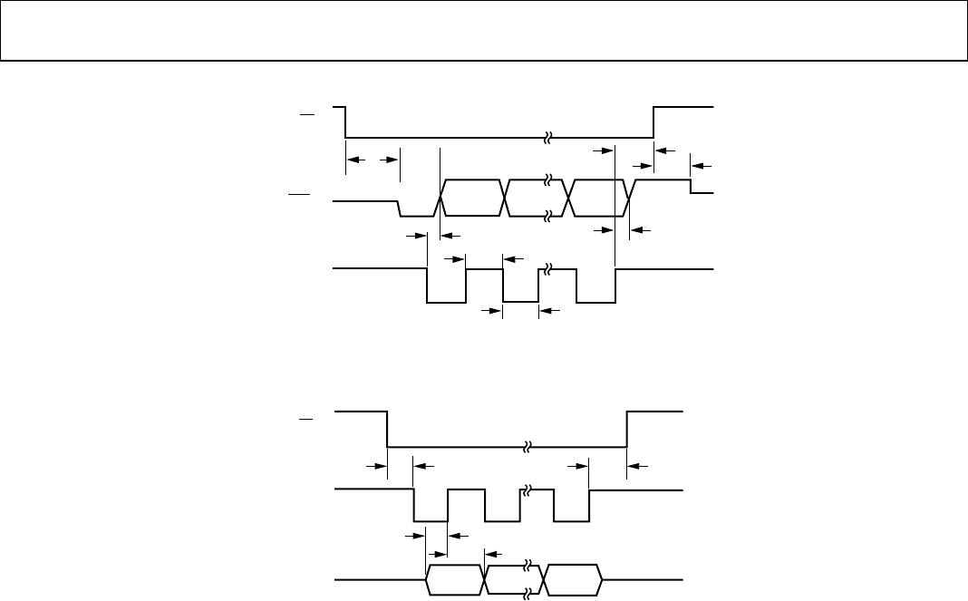
t
3
100 ns min SCLK high pulse width
t
4
100 ns min SCLK low pulse width
Read Operation
t
1
0 ns min
CS falling edge to DOUT/RDY active time
60 ns max DV
DD
= 4.75 V to 5.25 V
80 ns max DV
DD
= 2.7 V to 3.6 V
t
2
3
0 ns min SCLK active edge to data valid delay
4
60 ns max DV
DD
= 4.75 V to 5.25 V
80 ns max DV
DD
= 2.7 V to 3.6 V
t
5
5, 6
10 ns min
Bus relinquish time after
CS inactive edge
80 ns max
t
6
0 ns min
SCLK inactive edge to
CS inactive edge
t
7
10 ns min
SCLK inactive edge to DOUT/
RDY high
Write Operation
t
8
0 ns min
CS falling edge to SCLK active edge setup time
4
t
9
30 ns min Data valid to SCLK edge setup time
t
10
25 ns min Data valid to SCLK edge hold time
t
11
0 ns min
CS rising edge to SCLK edge hold time
1
Sample tested during initial release to ensure compliance. All input signals are specified with t
R
= t
F
= 5 ns (10% to 90% of DV
DD
) and timed from a voltage level of 1.6 V.
2
See Figure 3 and Figure 4.
3
These numbers are measured with the load circuit shown in Figure 2 and defined as the time required for the output to cross the V
OL
or V
OH
limits.
4
SCLK active edge is the falling edge of SCLK.
5
These numbers are derived from the measured time taken by the data output to change 0.5 V when loaded with the circuit shown in Figure 2. The measured number
is then extrapolated back to remove the effects of charging or discharging the 50 pF capacitor. This means that the times quoted in the timing characteristics are the
true bus relinquish times of the part and, as such, are independent of external bus loading capacitances.
6
RDY
returns high after a read of the ADC. In single conversion mode and continuous conversion mode, the same data can be read again, if required, while
RDY
is high,
although care should be taken to ensure that subsequent reads do not occur close to the next output update. In continuous read mode, the digital word can be read
only once.
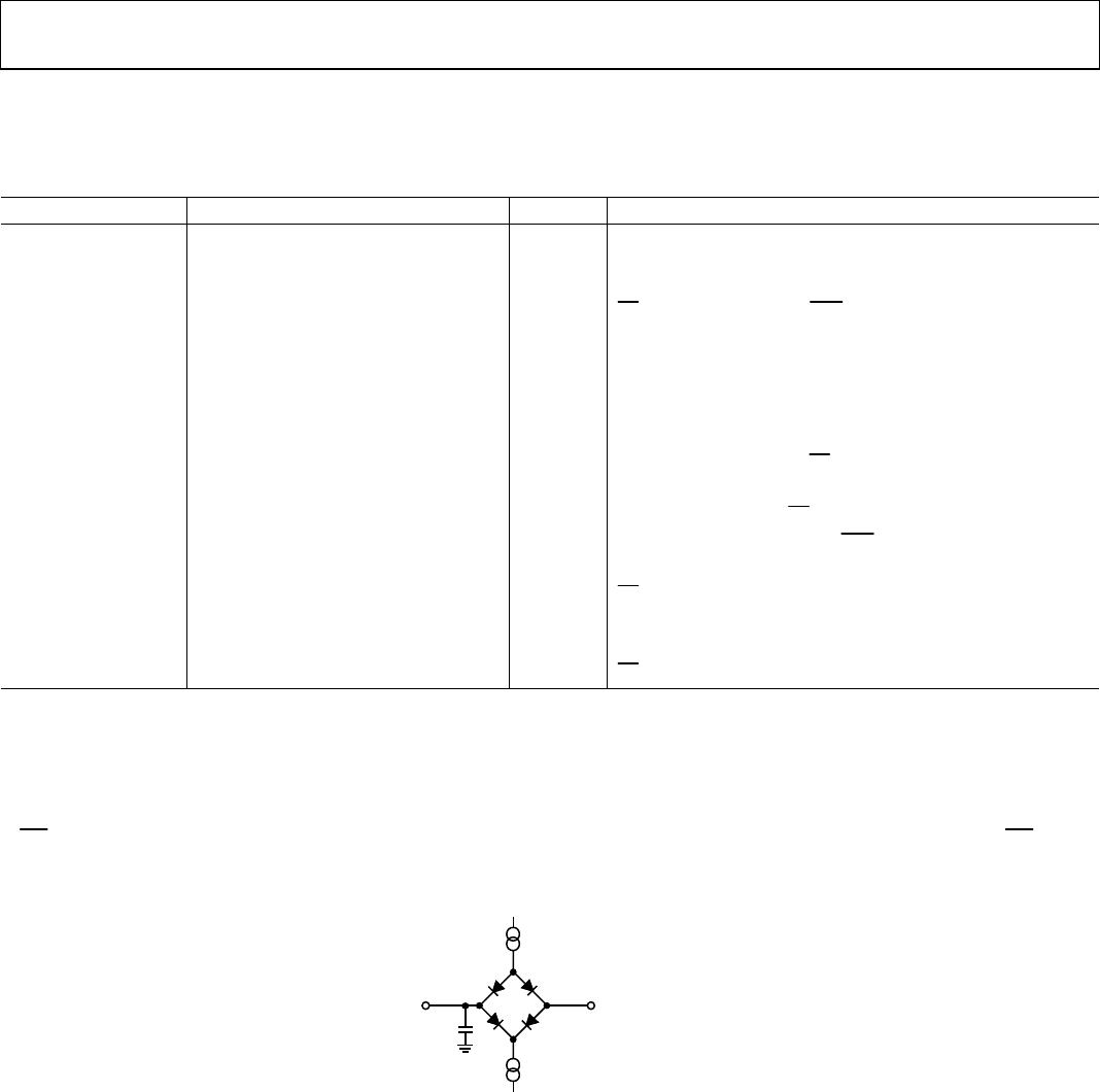
6721-002
I
SINK
(1.6mA WITH DV
DD
= 5V,
100µA WITH DV
DD
= 3V)
I
SOURCE
(200µA WITH DV
DD
= 5V,
100µA WITH DV
DD
= 3V)
1.6V
TO
OUTPUT
PIN
50pF
Figure 2. Load Circuit for Timing Characterization