AD7785
Rev. 0 | Page 22 of 32
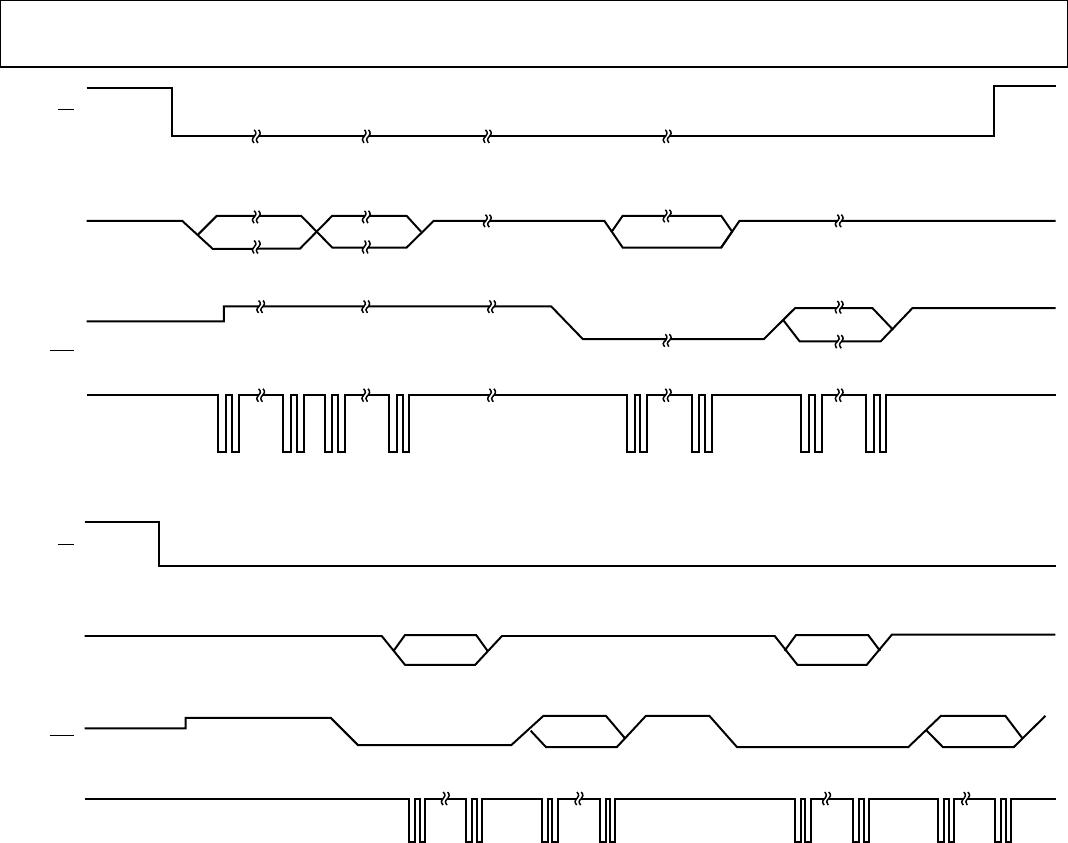
Figure 3 and Figure 4 show timing diagrams for interfacing to
the AD7785 with
CS
being used to decode the part. Figure 3
shows the timing for a read operation from the AD7785 output
shift register, and
Figure 4 shows the timing for a write opera-
tion to the input shift register. It is possible to read the same
word from the data register several times, even though the
DOUT/
RDY
line returns high after the first read operation.
However, care must be taken to ensure that the read operations
have been completed before the next output update occurs. In
continuous read mode, the data register can be read only once.
The serial interface can operate in 3-wire mode by tying
CS
low.
In this case, the SCLK, DIN, and DOUT/
RDY
lines are used
to communicate with the AD7785. The end of the conversion
can be monitored using the
RDY
bit in the status register. This
scheme is suitable for interfacing to microcontrollers. If
CS
is
required as a decoding signal, it can be generated from a port
pin. For microcontroller interfaces, it is recommended that
SCLK idle high between data transfers.
The AD7785 can be operated with
CS
being used as a frame
synchronization signal. This scheme is useful for DSP interfaces.
In this case, the first bit (MSB) is effectively clocked out by
CS
,
because
CS
would normally occur after the falling edge of SCLK
in DSPs. The SCLK can continue to run between data transfers,
provided the timing numbers are obeyed.
The serial interface can be reset by writing a series of 1s on the
DIN input. If a Logic 1 is written to the AD7785 line for at least
32 serial clock cycles, the serial interface is reset. This ensures
that the interface can be reset to a known state if the interface
gets lost due to a software error or some glitch in the system.
Reset returns the interface to the state in which it is expecting
a write to the communications register. This operation resets
the contents of all registers to their power-on values. Following
a reset, the user should allow a period of 500 μs before
addressing the serial interface.
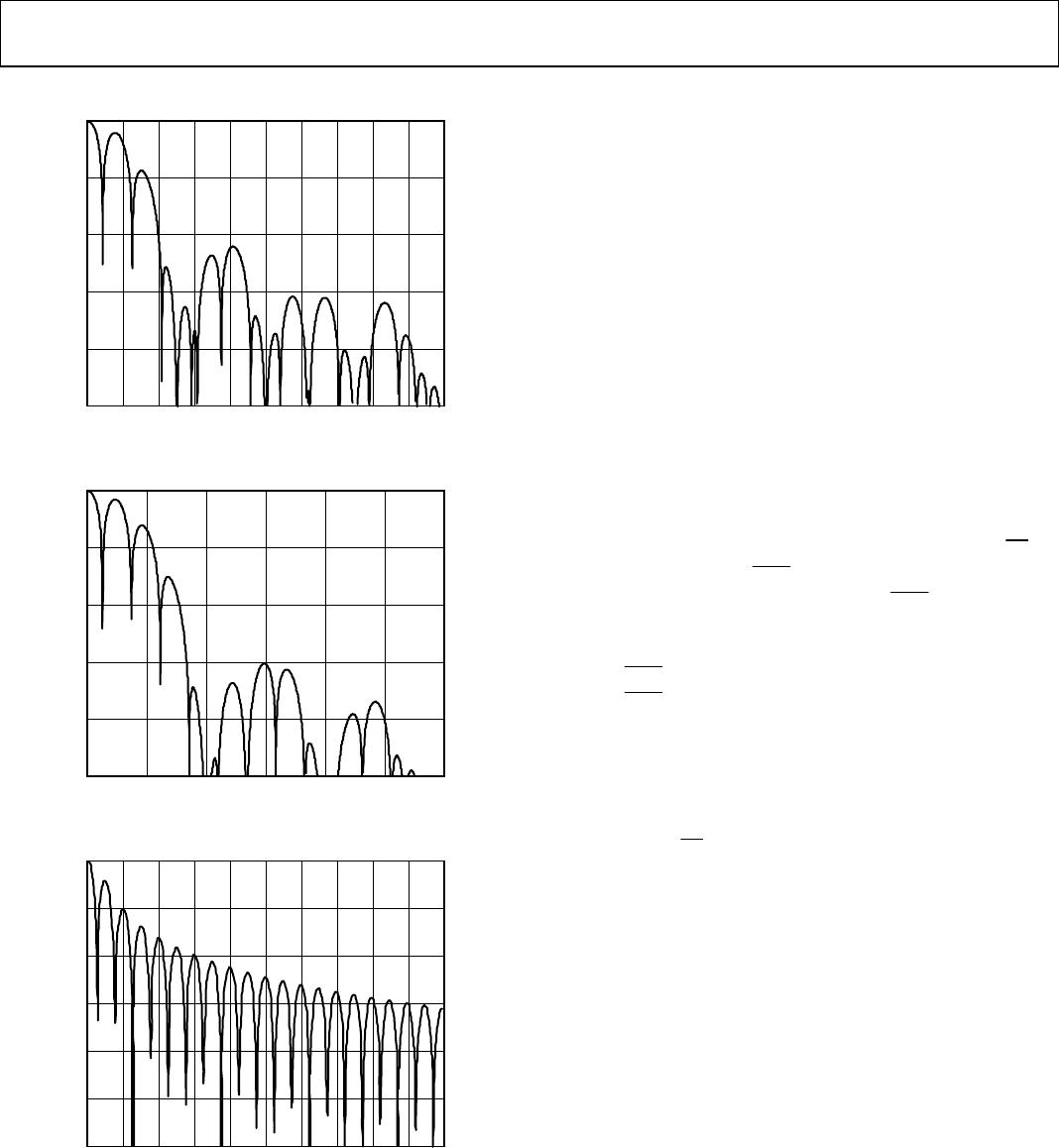
The AD7785 can be configured to continuously convert or to
perform a single conversion. See
Figure 17 through Figure 19.
Single Conversion Mode
In single conversion mode, the AD7785 is placed in shutdown
mode between conversions. When a single conversion is initi-
ated by setting MD2, MD1, MD0 to 0, 0, 1 in the mode register,
the AD7785 powers up, performs a single conversion, and then
returns to power-down mode. The on-chip oscillator requires
1 ms to power up. A conversion requires a time period of
2 × t
ADC
. DOUT/
RDY
goes low to indicate the completion of a
conversion. When the data-word has been read from the data
register, DOUT/
RDY
goes high. If
CS
is low, DOUT/
RDY
remains high until another conversion is initiated and com-
pleted. The data register can be read several times, if required,
even when DOUT/
RDY
has gone high.
Continuous Conversion Mode
This is the default power-up mode. The AD7785 continuously
converts, the
RDY
pin in the status register going low each time
a conversion is completed. If
CS
is low, the DOUT/
RDY
line
also goes low when a conversion is complete. To read a conver-
sion, the user writes to the communications register indicating
that the next operation is a read of the data register. The digital
conversion is placed on the DOUT/
RDY
pin as soon as SCLK
pulses are applied to the ADC. DOUT/
RDY
returns high when
the conversion is read. The user can read this register additional
times, if required. However, the user must ensure that the data
register is not being accessed at the completion of the next
conversion, otherwise the new conversion word is lost.