16
FN8172.4
August 29, 2006
D.C. OPERATING CHARACTERISTICS (Over the recommended operating conditions unless otherwise specified.)
ENDURANCE AND DATA RETENTION
CAPACITANCE
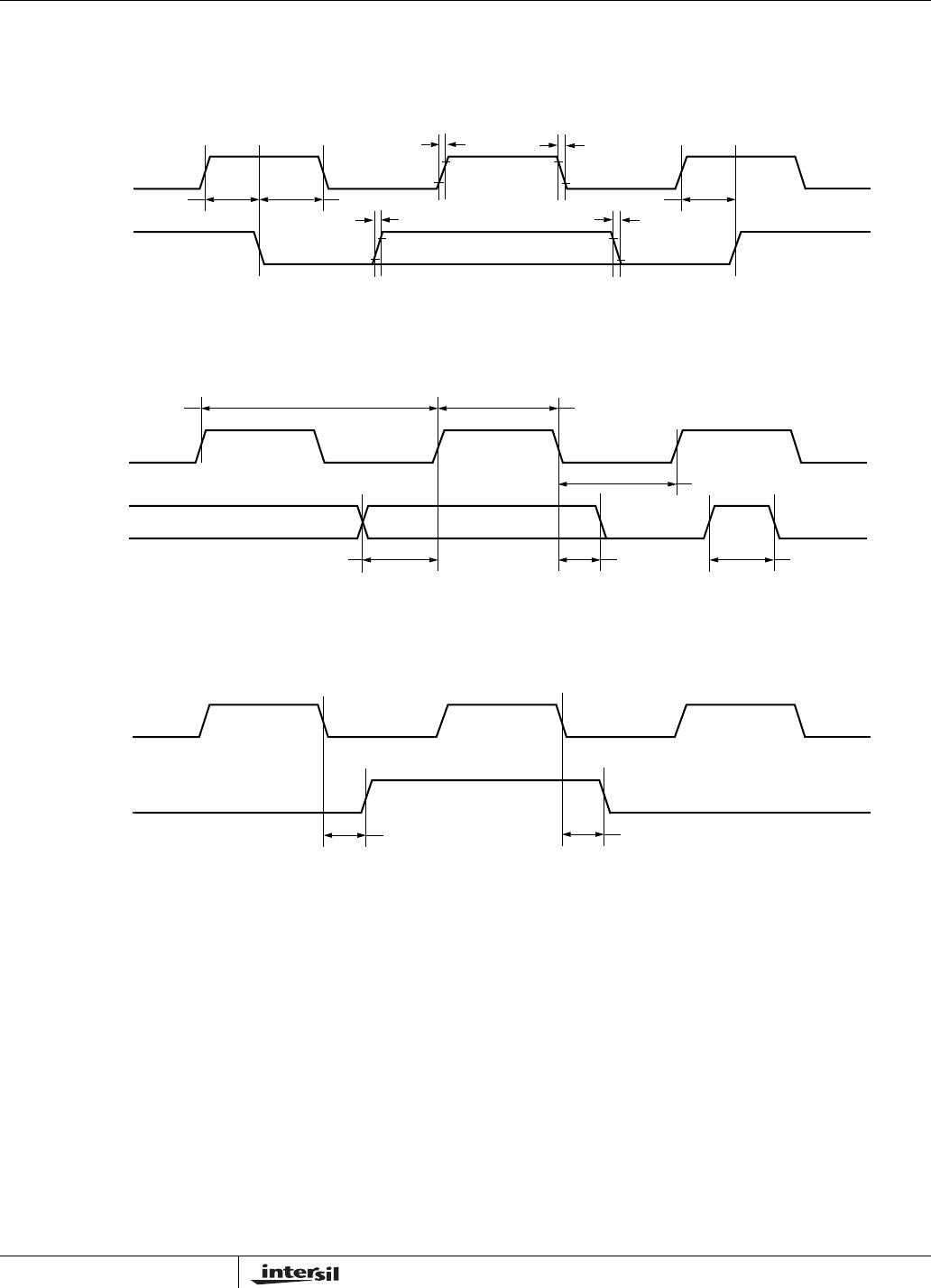
POWER-UP TIMING
POWER-UP AND DOWN REQUIREMENTS
The are no restrictions on the sequencing of the bias supplies V
CC
, V+, and V- provided that all three supplies reach
their final values within 1msec of each other. At all times, the voltages on the potentiometer pins must be less than V+
and more than V-. The recall of the wiper position from nonvolatile memory is not in effect until all supplies reach their
final value. The V
CC
ramp rate spec is always in effect.
A.C. TEST CONDITIONS
Notes: (6) This parameter is not 100% tested
(7) t
PUR
and t
PUW
are the delays required from the time the (last) power supply (V
CC
-) is stable until the specific instruction can be issued.
These parameters are periodically sampled and not 100% tested.
Symbol Parameter Test Conditions Min. Typ. Max. Units
I
CC1
V
CC
supply current
(active)
f
SCL
= 400kHz; V
CC
= +6V;
SDA = Open; (for 2-Wire, Active, Read and
Volatile Write States only)
3mA
I
CC2
V
CC
supply current
(nonvolatile write)
f
SCL
= 400kHz; V
CC
= +6V;
SDA = Open; (for 2-Wire, Active,
Nonvolatile Write State only)
5mA
I
SB
V
CC
current (standby) VCC = +6V; VIN = VSS or VCC;
SDA = VCC; (for 2-Wire, Standby State only)
5 µA
I
LI
Input leakage current V
IN
= V
SS
to V
CC
10 µA
I
LO
Output leakage current V
OUT
= V
SS
to V
CC
10 µA
V
IH
Input HIGH voltage V
CC
x 0.7 V
CC
+ 1 V
V
IL
Input LOW voltage -1 V
CC
x 0.3 V
V
OL
Output LOW voltage I
OL
= 3mA 0.4 V
V
OH
Output HIGH voltage
Parameter Min. Units
Minimum endurance 100,000 Data changes per bit per register
Data retention 100 years
Symbol Test Max. Units Test Conditions
C
IN/OUT
(6)
Input / Output capacitance (SDA) 8 pF V
OUT
= 0V
C
IN
(6)
Input capacitance (SCL, WP, A3, A2, A1 and A0)6 pF V
IN
= 0V
Symbol Parameter Min. Max. Units
t
r
V
CC
(6)
V
CC
Power-up rate
0.2 50 V/ms
t
PUR
(7)
Power-up to initiation of read operation 1 ms
Input Pulse Levels
V
CC
x 0.1 to V
CC
x 0.9
Input rise and fall times 10ns
Input and output timing level
V
CC
x 0.5
X9268