8
FN8172.4
August 29, 2006
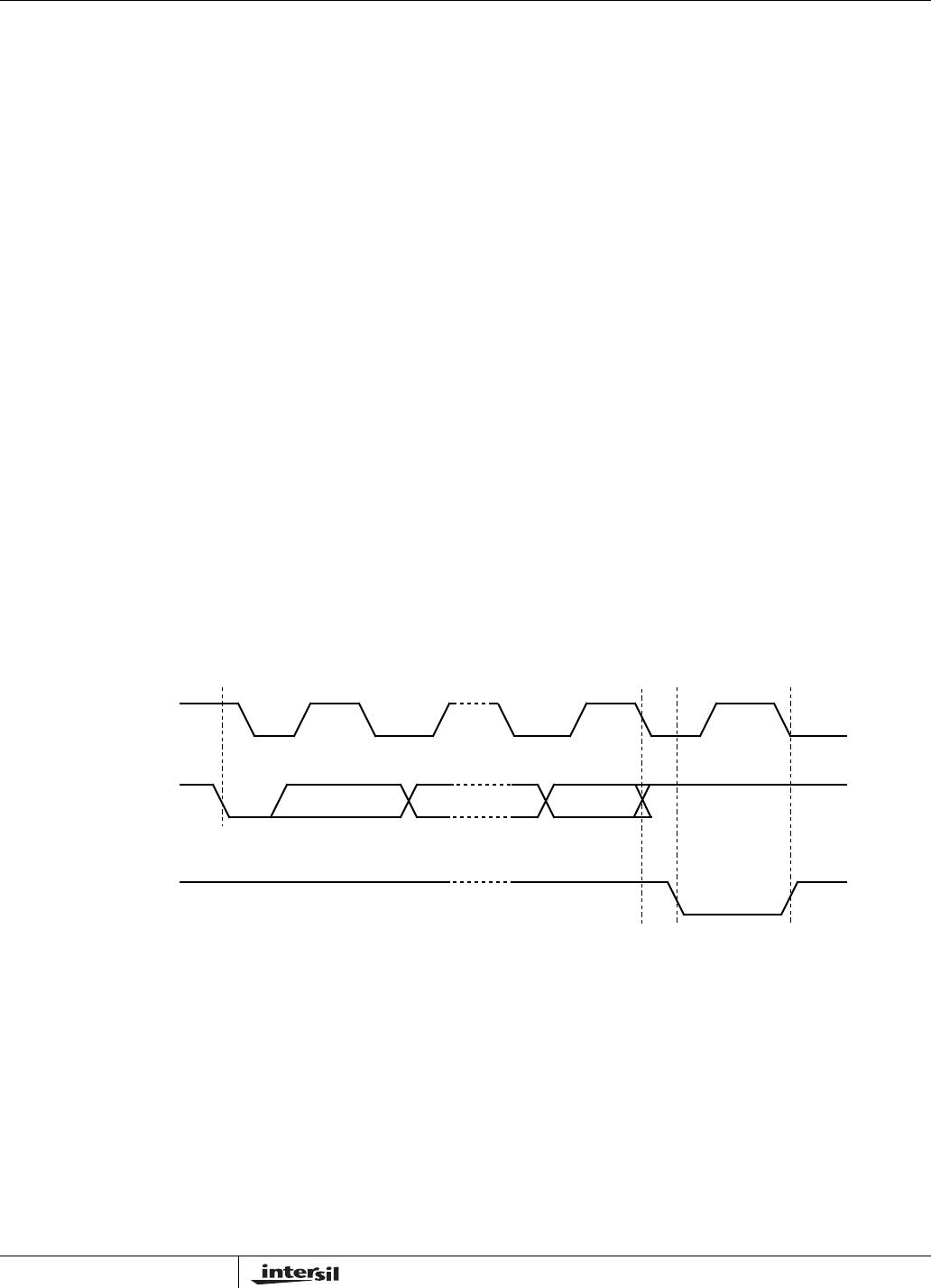
Acknowledge Polling
The disabling of the inputs, during the internal
nonvolatile write operation, can be used to take
advantage of the typical 5ms nonvolatile write cycle
time. Once the stop condition is issued to indicate the
end of the nonvolatile write command the X9268
initiates the internal write cycle. ACK polling, Flow 1,
can be initiated immediately. This involves issuing the
start condition followed by the device slave address. If
the X9268 is still busy with the write operation no ACK
will be returned. If the X9268 has completed the write
operation an ACK will be returned and the master can
then proceed with the next operation.
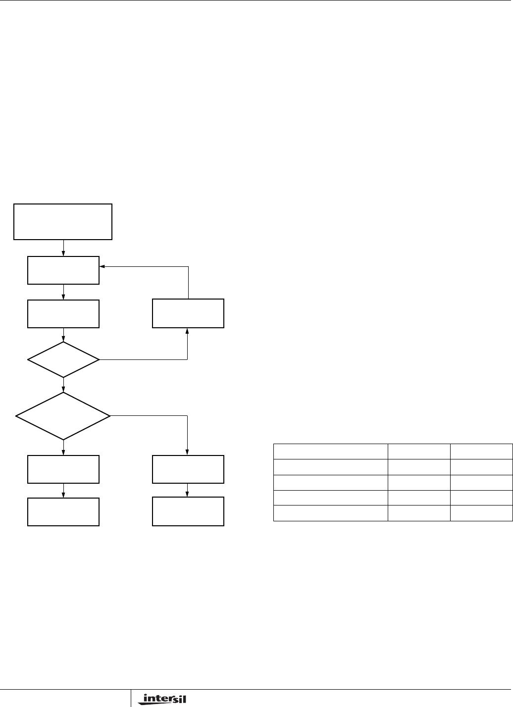
FLOW 1: ACK Polling Sequence
INSTRUCTION AND REGISTER DESCRIPTION
Instructions
D
EVICE ADDRESSING: IDENTIFICATION BYTE (ID AND A)
The first byte sent to the X9268 from the host is called
the Identification Byte. The most significant four bits of
the slave address are a device type identifier. The
ID[3:0] bits is the device id for the X9268; this is fixed
as 0101[B] (refer to Table 1).
The A[3:0] bits in the ID byte is the internal slave
address. The physical device address is defined by
the state of the A3 - A0 input pins. The slave address
is externally specified by the user. The X9268
compares the serial data stream with the address
input state; a successful compare of both address
bits is required for the X9268 to successfully continue
the command sequence. Only the device which slave
address matches the incoming device address sent
by the master executes the instruction. The A3 - A0
inputs can be actively driven by CMOS input signals
or tied to V
CC
or V
SS
.
I
NSTRUCTION BYTE (I)
The next byte sent to the X9268 contains the
instruction and register pointer information. The three
most significant bits are used provide the instruction
opcode I [3:0]. The RB and RA bits point to one of the
four Data Registers of each associated XDCP. The
least significant bit points to one of two Wiper Counter
Registers or Pots. The format is shown in Table 2.
Register Selection
Nonvolatile Write
Command Completed
EnterACK Polling
Issue
START
Issue Slave
Address
ACK
Returned?
Further
Operation?
Issue
Instruction
Issue STOP
No
Yes
Yes
Proceed
Issue STOP
No
Proceed
Register Selected RB RA
DR0 0 0
DR1 0 1
DR2 1 0
DR3 1 1
X9268