Expand menu
Hello, Sign in
My Account
0
Cart
Home
Products
Sensors
Semiconductors
Passive Components
Connectors
Power
Electromechanical
Optoelectronics
Circuit Protection
Integrated Circuits - ICs
Main Products
Manufacturers
Blog
Services
About OMO
About Us
Contact Us
Check Stock
X9268TS24IZ-2.7T1
P1-P3
P4-P6
P7-P9
P10-P12
P13-P15
P16-P18
P19-P21
P22-P22
19
FN8172.4
August 29, 2006
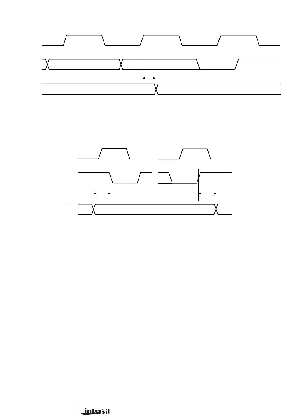
XDCP Timing (for All Load Instructions)
Write Protect a
nd Device Address Pins
Timing
SCL
SDA
VWx
(STOP)
LSB
t
WRL
SDA
SCL
...
...
...
WP
A0, A1
t
SU:WPA
t
HD:WPA
(START)
(STOP)
(Any Instruction)
X9268
20
FN8172.4
August 29, 2006
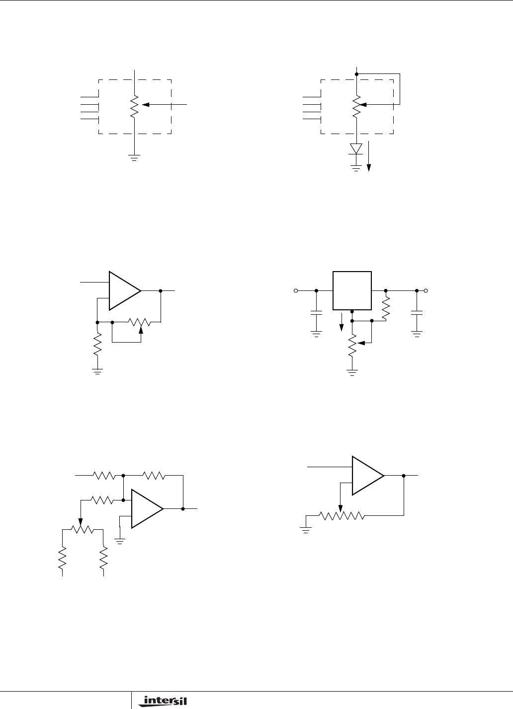
APPLICATIONS INFORMATION
Basic Conf
igurations o
f Electronic
Potentiomete
rs
Application Circuits
V
R
RW
+V
R
I
Three terminal Po
tentiometer;
Variable voltage divider
Two terminal Variable Resistor;
Variable current
Noninverting Amplifier
Voltage Regulator
Offset Voltage Adjustment
Comparator with Hysterisis
+
–
V
S
V
O
R
2
R
1
V
O
= (1+R
2
/R
1
)V
S
R
1
R
2
I
adj
V
O
(REG) = 1.25V (1+R
2
/R
1
)+I
adj
R
2
V
O
(REG)
V
IN
317
+
–
V
S
V
O
R
2
R
1
V
UL
= {R
1
/(R
1
+R
2
)} V
O
(max)
V
LL
= {R
1
/(R
1
+R
2
)} V
O
(min)
100k
Ω
10k
Ω
10k
Ω
10k
Ω
-12V
+12V
TL072
+
–
V
S
V
O
R
2
R
1
}
}
X9268
21
FN8172.4
August 29, 2006
Application Circuits (continued)
Attenuator
Filter
Inverting Amplifier
Equivalent L-R Circuit
+
–
V
S
V
O
R
3
R
1
V
O
= G V
S
-1/2
≤
G
≤
+1/2
G
O
= 1 + R
2
/R
1
fc = 1/(2
π
RC)
+
–
V
S
V
O
R
2
R
1
Z
IN
= R
2
+ s R
2
(R
1
+ R
3
) C
1
= R
2
+ s Leq
(
R
1
+ R
3
) >> R
2
+
–
V
S
Function Generator
R
2
R
4
R
1
= R
2
= R
3
= R
4
= 10k
Ω
+
–
V
S
R
2
R
1
R
C
}
}
V
O
= G V
S
G = - R
2
/R
1
R
2
C
1
R
1
R
3
Z
IN
+
–
R
2
+
–
R
1
}
}
R
A
R
B
frequency
∝
R
1
, R
2
, C
amplitude
∝
R
A
, R
B
C
V
O
X9268
P1-P3
P4-P6
P7-P9
P10-P12
P13-P15
P16-P18
P19-P21
P22-P22
X9268TS24IZ-2.7T1
Mfr. #:
Buy X9268TS24IZ-2.7T1
Manufacturer:
Renesas / Intersil
Description:
Digital Potentiometer ICs DL DCP 100KOHM 256 TAPS 2-WIRE
Lifecycle:
New from this manufacturer.
Delivery:
DHL
FedEx
Ups
TNT
EMS
Payment:
T/T
Paypal
Visa
MoneyGram
Western
Union
Products related to this Datasheet
X9268TS24IZ-2.7
X9268US24IZ
X9268TS24IZT1
X9268TS24Z-2.7
X9268US24ZT1
X9268TS24Z
X9268TS24IZ-2.7T1
X9268TS24IZ
X9268US24IZ-2.7
X9268TS24ZT1
X9268US24IZT1
X9268US24IZ-2.7T1
X9268TS24Z-2.7T1
X9268US24Z-2.7T1
X9268US24Z-2.7
X9268US24Z
X9268TS24
X9268TS24-2.7
X9268TS24I
X9268TS24T1
X9268US24
X9268US24-2.7
X9268US24T1