General Description
The MAX2160/EBG tuner ICs are designed for use in
Japanese mobile digital TV (ISDB-T single-segment)
applications. The devices directly convert UHF band
signals to a low-IF using a broadband I/Q downconvert-
er. The operating frequency range extends from
470MHz to 770MHz.
The MAX2160/EBG support both I/Q low-IF interfaces
as well as single low-IF interfaces, making the devices
universal tuners for various digital demodulator IC
implementations.
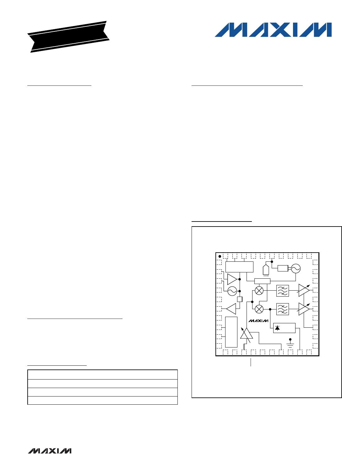
The MAX2160/EBG include an LNA, RF variable-gain
amplifiers, I and Q downconverting mixers, low-IF variable-
gain amplifiers, and bandpass filters providing in excess of
42dB of image rejection. The parts are capable of operat-
ing with either high-side or low-side local oscillator (LO)
injection. The MAX2160/EBG’s variable-gain amplifiers pro-
vide in excess of 100dB of gain-control range.
The MAX2160/EBG also include fully monolithic VCOs
and tank circuits, as well as a complete frequency syn-
thesizer. The devices include a XTAL oscillator as well
as a separate TCXO input buffer. The devices operate
with XTAL/TCXO oscillators from 13MHz to 26MHz
allowing the shared use of a VC-TCXO in cellular hand-
set applications. Additionally, a divider is provided for
the XTAL/TCXO oscillator allowing for simple and low-
cost interfacing to various channel decoders.
The MAX2160/EBG are specified for operation from
-40°C to +85°C and available in a 40-pin (6mm x 6mm)
thin QFN lead-free plastic package with exposed pad-
dle (EP), and in a 3.175mm x 3.175mm lead-free wafer-
level package (WLP).
Applications
Cell Phone Mobile TVs
Personal Digital Assistants (PDAs)
Pocket TVs
Features
Low Noise Figure: < 4dB Typical
High Dynamic Range: -98dBm to 0dBm
High-Side or Low-Side LO Injection
Integrated VCO and Tank Circuits
Low LO Phase Noise: Typical -88dBc/Hz at 10kHz
Integrated Frequency Synthesizer
Integrated Bandpass Filters
52dB Typical Image Rejection
Single +2.7V to +3.3V Supply Voltage
Three Low-Power Modes
Two-Wire, I
2
C-Compatible Serial Control Interface
Very Small Lead-Free WLP Package
MAX2160/MAX2160EBG
ISDB-T Single-Segment Low-IF Tuners
________________________________________________________________ Maxim Integrated Products 1
PART TEMP RANGE PIN-PACKAGE
MAX2160ETL -40°C to +85°C 40 Thi n QFN - E P *
MAX2160ETL+ -40°C to +85°C 40 Thi n QFN - E P *
MAX2160EBG+ -40°C to +85°C W LP
Ordering Information
19-0068; Rev 5; 10/09
For pricing, delivery, and ordering information, please contact Maxim Direct at 1-888-629-4642,
or visit Maxim’s website at www.maxim-ic.com.
+Denotes a lead(Pb)-free/RoHS-compliant package.
*EP = Exposed paddle.
EVALUATION KIT
AVAILABLE
N.C.
VCCBB
QOUT
GNDBB
GC2
ENTCXO
N.C.
IOUT
N.C.
N.C.
XTAL
GNDXTAL
VCCXTAL
XTALOUT
÷
VCCDIG
SDA
SCL
LTC
TCXO
N.C.
40 39 38 37 36 35 34 33 32 31
11 12 13 14 15 16 17 18 19 20
1
2
3
4
5
6
7
8
9
10
30
29
28
27
26
25
24
23
22
21
N.C.
VCCLNA
GC1
PWRDET
VCCFLT
SHDN
RFIN
VCCBIAS
N.C.
VCCCP
CPOUT
TEST
GNDTUNE
VTUNE
GNDVCO
VCCVCO
VCOBYP
N.C.
GNDCP
VCCMX
TOP VIEW
DIV4
EP
MAX2160
FREQUENCY
SYNTHESIZER
INTERFACE LOGIC
AND CONTROL
TANK
PWRDET
ADC
TQFN
Pin Configurations/
Functional Diagrams
Pin Configurations/Functional Diagrams continued at end of
data sheet.
MAX2160/MAX2160EBG
ISDB-T Single-Segment Low-IF Tuners
2 _______________________________________________________________________________________
ABSOLUTE MAXIMUM RATINGS
DC ELECTRICAL CHARACTERISTICS
(MAX2160 EV kit, V
CC
= +2.7V to +3.3V, V
GC1
= V
GC2
= 0.3V (maximum gain), no RF input signals at RFIN, baseband I/Os are open
circuited and VCO is active with f
LO
= 767.714MHz, registers set according to the recommended default register conditions of
Tables 2–11, T
A
= -40°C to +85°C, unless otherwise noted. Typical values are at V
CC
= +2.85V, T
A
= +25°C, unless otherwise
noted.) (Note 1)
Stresses beyond those listed under “Absolute Maximum Ratings” may cause permanent damage to the device. These are stress ratings only, and functional
operation of the device at these or any other conditions beyond those indicated in the operational sections of the specifications is not implied. Exposure to
absolute maximum rating conditions for extended periods may affect device reliability.
All VCC_ Pins to GND............................................-0.3V to +3.6V
All Other Pins to GND.................................-0.3V to (V
CC
+ 0.3V)
RFIN, Maximum RF Input Power ....................................+10dBm
ESD Rating...........................................................................±1kV
Short-Circuit Duration
IOUT, QOUT, CPOUT, XTALOUT, PWRDET, SDA,
TEST, LTC, VCOBYP ...........................................................10s
Continuous Power Dissipation (T
A
= +70°C)
40-Pin Thin QFN (derate 35.7mW/°C above +70°C)....2857mW
WLP (derate 10.8mW/°C above +70°C).........................704mW
Operating Temperature Range ...........................-40°C to +85°C
Junction Temperature......................................................+150°C
Storage Temperature Range .............................-65°C to +150°C
Lead Temperature (soldering, 10s) .................................+300°C
PARAMETER CONDITIONS MIN TYP MAX UNITS
SUPPLY
Supply Voltage 2.7 2.85 3.3 V
Receive mode, SHDN = V
CC
, BBL[1:0] = 00 44 53.5
Standby mode, bit STBY = 1 2 4
mA
Power-down mode, bit PWDN = 1, EPD = 0 5 40
Supply Current (See Tables 15
and 16)
Shutdown mode, SHDN = GND 0 10
µA
ANALOG GAIN-CONTROL INPUTS (GC1, GC2)
Input Voltage Range Maximum gain = 0.3V 0.3 2.7 V
Input Bias Current -15 +15 µA
VCO TUNING VOLTAGE INPUT (VTUNE)
Input Voltage Range 0.4 2.3 V
VTUNE ADC
Resolution 3 bits
Input Voltage Range 0.3 2.4 V
110 to 111 V
CC
- 0.4
101 to 110 1.9
100 to 101 1.7
011 to 100 1.3
010 to 011 0.9
001 to 010 0.6
Reference Ladder Trip Point ADC read bits
000 to 001 0.4
V
LOCK TIME CONSTANT OUTPUT (LTC)
Bit LTC = 0 1
Source Current
Bit LTC = 1 2
µA
CAUTION! ESD SENSITIVE DEVICE
MAX2160/MAX2160EBG
ISDB-T Single-Segment Low-IF Tuners
_______________________________________________________________________________________ 3
DC ELECTRICAL CHARACTERISTICS (continued)
(MAX2160 EV kit, V
CC
= +2.7V to +3.3V, V
GC1
= V
GC2
= 0.3V (maximum gain), no RF input signals at RFIN, baseband I/Os are open
circuited and VCO is active with f
LO
= 767.714MHz, registers set according to the recommended default register conditions of
Tables 2–11, T
A
= -40°C to +85°C, unless otherwise noted. Typical values are at V
CC
= +2.85V, T
A
= +25°C, unless otherwise
noted.) (Note 1)
PARAMETER CONDITIONS MIN TYP MAX UNITS
SHUTDOWN CONTROL (SHDN)
Input-Logic-Level High 0.7 x V
CC
V
Input-Logic-Level Low 0.3 x V
CC
V
2-WIRE SERIAL INPUTS (SCL, SDA)
Clock Frequency 400 kHz
Input-Logic-Level High 0.7 x V
CC
V
Input-Logic-Level Low 0.3 x V
CC
V
Input Leakage Current Digital inputs = GND or V
CC
±0.1 ±1 µA
2-WIRE SERIAL OUTPUT (SDA)
Output-Logic-Level Low 0.2 V
AC ELECTRICAL CHARACTERISTICS
(MAX2160 EV kit, V
CC
= +2.7V to +3.3V, f
RF
= 767.143MHz, f
LO
= 767.714MHz, f
BB
= 571kHz, f
XTAL
= 16MHz, V
GC1
= V
GC2
= 0.3V
(maximum gain), registers set according to the recommended default register conditions of Tables 2–11, RF input signals as speci-
fied, baseband output load as specified, T
A
= -40°C to +85°C, unless otherwise noted. Typical values are at V
CC
= +2.85V,
T
A
= +25°C, unless otherwise noted.) (Note 1)
PARAMETER CONDITIONS MIN TYP MAX UNITS
MAIN SIGNAL PATH PERFORMANCE
Input Frequency Range 470 770 MHz
Minimum Input Signal 13-segment input -98 dBm
Maximum Voltage Gain CW tone, V
GC1
= V
GC2
= 0.3V, bit MOD = 1 102 dB
Minimum Voltage Gain CW tone, V
GC1
= V
GC2
= 2.7V, bit MOD = 0 4 dB
RF Gain-Control Range 0.3V < V
GC1
< 2.7V 38 43 dB
Baseband Gain-Control Range 0.3V < V
GC2
< 2.7V 57 67 dB
In-Band Input IP3 (Note 2) +4 dBm
Out-of-Band Input IP3 (Note 3) +16.7 dBm
Input IP2 (Note 4) +16 dBm
Input P
1dB
CW tone, V
GC1
= V
GC2
= 2.7V, bit MOD = 0 0 dBm
Noise Figure V
GC1
= V
GC2
= 0.3V, T
A
= +25°C (Note 5) 3.8 5 dB
Image Rejection 42 52 dB
Minimum RF Input Return Loss f
RF
= 620MHz, 50 system 14 dB
LO Leakage at RFIN -100 dBm
IF POWER DETECTOR
Resolution 3 bits
Minimum RF Attack Point Power at RFIN -62 dBm
Maximum RF Attack Point Power at RFIN -48 dBm
Detector Bandwidth 3dB RF bandwidth ±35 MHz
Output Compliance Range 0.3 2.7 V
Response Time C
14
= 10nF 0.1 ms

MAX2160ETL+T

Mfr. #:
Manufacturer:
Maxim Integrated
Description:
Tuners ISDB-T Single-Seg Low-IF Tuner
Lifecycle:
New from this manufacturer.
Delivery:
DHL FedEx Ups TNT EMS
Payment:
T/T Paypal Visa MoneyGram Western Union