MAX2160/MAX2160EBG
ISDB-T Single-Segment Low-IF Tuners
10 ______________________________________________________________________________________
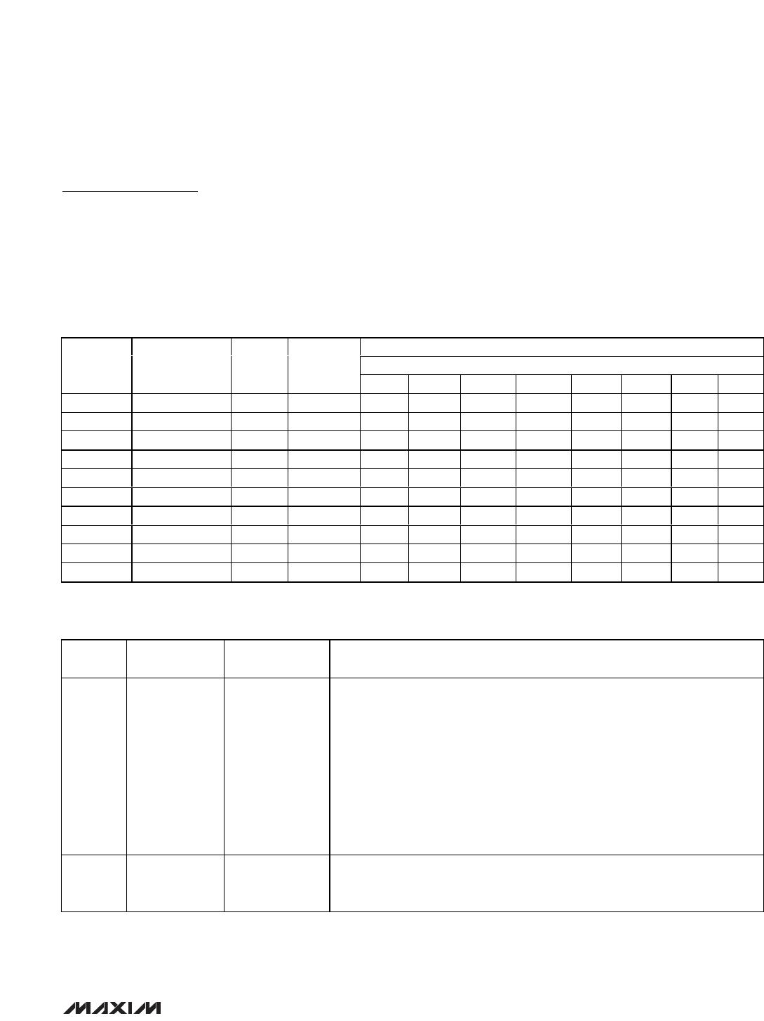
Pin Description (continued)
PIN BUMP NO.
TQFN WLP
NAME DESCRIPTION
20 39 VCCFLT
DC Power Supply for Baseband Filter Circuits. Connect to a +2.85V low-noise
supply. Bypass to GND with a 100pF capacitor connected as close to the pin as
possible. Do not share capacitor ground vias with other ground connections.
22 37 ENTCXO
XTAL/TCXO Select. Logic-high enables the TCXO input and disables the XTAL input.
Logic-low disables the TCXO input and enables the XTAL input. This pin is internally
pulled up to V
CC
.
23 47 GC2
Baseband Gain-Control Input. High-impedance analog input, with a 0.3V to 2.7V
operating range. V
GC2
= 0.3V corresponds to the maximum gain setting.
25 44 IOUT In-Phase Low-IF Output. Requires a DC-blocking capacitor.
26 — GNDBB Ground for Baseband Circuits. Connect to the PC board ground plane.
27 43 QOUT Quadrature Low-IF Output. Requires a DC-blocking capacitor.
29 41 VCCBB
DC Power Supply for Baseband Circuits. Connect to a +2.85V low-noise supply.
Bypass to GND with a 100pF capacitor connected as close to the pin as possible.
Do not share capacitor ground vias with other ground connections.
32 30 VCOBYP
Internal VCO Bias Bypass. Bypass directly to GNDVCO with a 470nF capacitor
connected as close to the pin as possible. Do not share capacitor ground vias with
other ground connections. See the Layout Considerations section.
33 26 VCCVCO
DC Power Supply for VCO Circuits. Connect to a +2.85V low-noise supply. Bypass
directly to GNDVCO with a 100pF capacitor connected as close to the pin as
possible. Do not share capacitor ground vias with other ground connections.
34 23 GNDVCO
VCO Circuit Ground. Connect to the PC board ground plane. See the Layout
Considerations section.
35 32 VTUNE
High-Impedance VCO Tune Input. Connect the PLL loop filter output directly to this
pin with the shortest connection as possible.
36 20 GNDTUNE
Ground for VTUNE. Connect to the PC board ground plane. See the Layout
Considerations section.
37 18 TEST Test Output. Used as a test output for various internal blocks. See Table 2.
38 16 CPOUT
Charge-Pump Output. Connect this output to the PLL loop filter input with the
shortest connection possible.
39 10 VCCCP
DC Power Supply for Charge-Pump Circuits. Connect to a +2.85V low-noise supply.
Bypass to GND with a 100pF capacitor connected as close to the pin as possible.
Do not share capacitor ground vias with other ground connections.
40 1 GNDCP
Charge-Pump Circuit Ground. Connect to the PC board ground plane. See the
Layout Considerations section.
EP — GND
Exposed Paddle (TQFN Only). Solder evenly to the board’s ground plane for proper
operation.
—
3, 6, 8, 13, 15,
27, 31, 40, 42
GND Ground. Connect to the PC board ground plane.
— 21 GNDLNA Ground for LNA. Connect to ground with trace.