MAX2160/MAX2160EBG
ISDB-T Single-Segment Low-IF Tuners
_______________________________________________________________________________________ 5
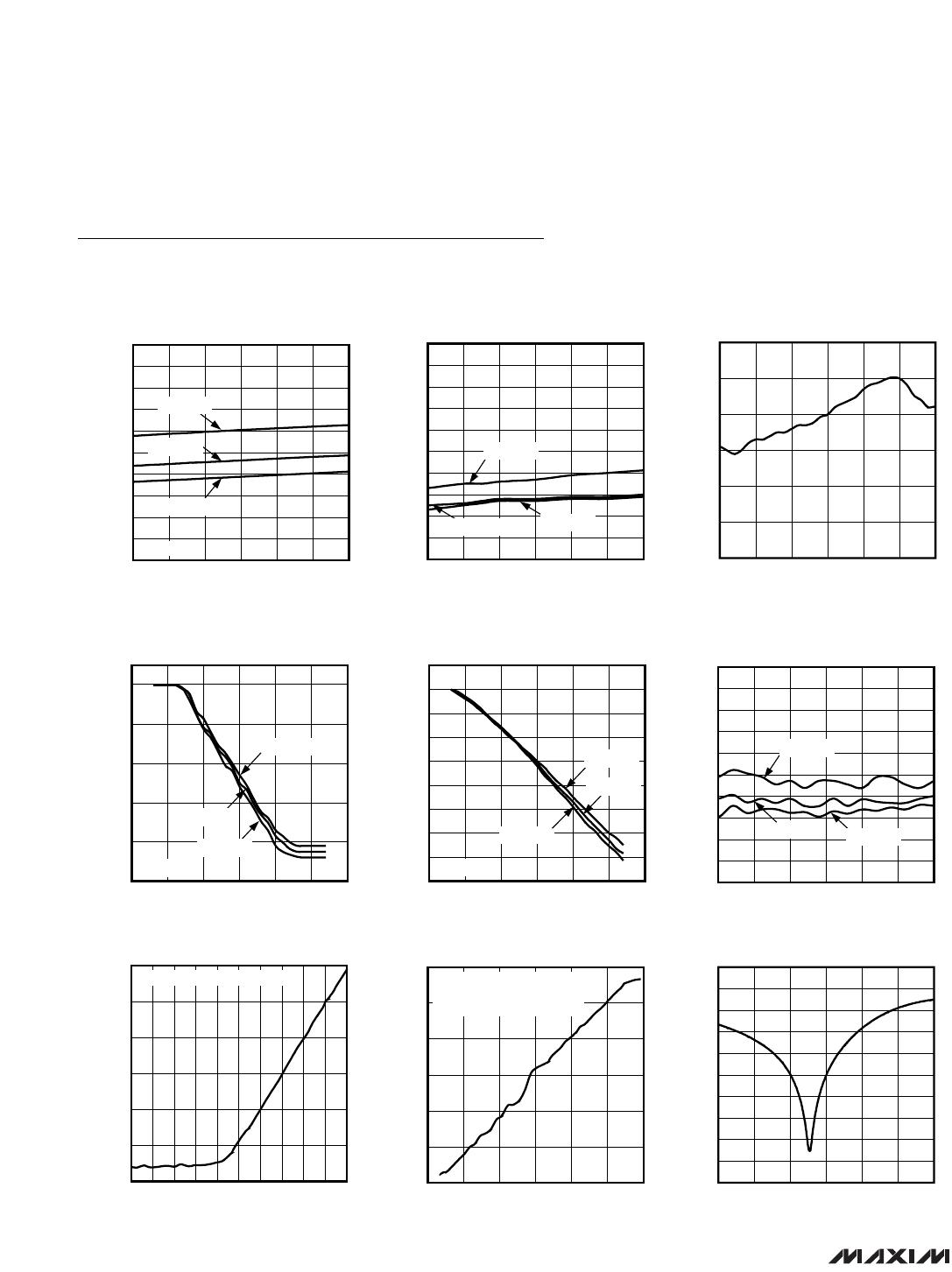
AC ELECTRICAL CHARACTERISTICS (continued)
(MAX2160 EV kit, V
CC
= +2.7V to +3.3V, f
RF
= 767.143MHz, f
LO
= 767.714MHz, f
BB
= 571kHz, f
XTAL
= 16MHz, V
GC1
= V
GC2
= 0.3V
(maximum gain), registers set according to the recommended default register conditions of Tables 2–11, RF input signals as speci-
fied, baseband output load as specified, T
A
= -40°C to +85°C, unless otherwise noted. Typical values are at V
CC
= +2.85V,
T
A
= +25°C, unless otherwise noted.) (Note 1)
PARAMETER CONDITIONS MIN TYP MAX UNITS
VOLTAGE-CONTROLLED OSCILLATOR AND LO GENERATION
Guaranteed VCO Frequency
Range
T
A
= -40°C to +85°C 1880 3080 MHz
Guaranteed LO Frequency
Range
T
A
= -40°C to +85°C 470 770 MHz
Tuning Voltage Range 0.4 2.3 V
f
OFFSET
= 1kHz -80
f
OFFSET
= 10kHz -87.5
f
OFFSET
= 100kHz -107
LO Phase Noise
0.4V < VTUNE < 2.3V,
T
A
= -40°C to +85°C
f
OFFSET
= 1MHz -128
dBc/Hz
XTAL OSCILLATOR INPUT (TCXO AND XTAL)
XTAL Oscillator Frequency
Range
Parallel resonance mode crystal 13 26 MHz
XTAL Minimum Negative
Resistance
16MHz < f
XTAL
< 18MHz (Note 5) 885 Ω
XTAL Nominal Input Capacitance 13.3 pF
TCXO Input Level AC-coupled sine-wave input 0.4 1.5 V
P-P
TCXO Minimum Input Impedance 10 kΩ
REFERENCE OSCILLATOR BUFFER OUTPUT (XTALOUT)
Output Frequency Range 1 26 MHz
Output-Buffer Divider Range 1 26
Output-Voltage Swing 0.7 V
P-P
Output Load 200 || 4 kΩ || pF
Output Duty Cycle 50 %
Output Impedance 160 Ω
Note 1: Min and max values are production tested at T
A
= +25°C and +85°C. Min and max limits at T
A
= -40°C are guaranteed by
design and characterization. Default register settings are not production tested; load all registers no sooner than 100µs
after power-up.
Note 2: In-band IIP3 is measured with two tones at f
LO
- 100kHz and f
LO
- 200kHz at a power level of -23dBm/tone. GC1 is set for
maximum attenuation (V
GC1
= 2.7V) and GC2 is adjusted to achieve 250mV
P-P
/tone at the I/Q outputs for an input desired
level of -23dBm.
Note 3: Out-of-band IIP3 is measured with two tones at f
RF
+ 6MHz and f
RF
+ 12MHz at a power level of -15dBm/tone. GC1 is set
for maximum attenuation (V
GC1
= 2.7V) and GC2 is adjusted to achieve 0.5V
P-P
at the I/Q outputs for an input desired level
of -50dBm. f
RF
is set to 767MHz + 1/7MHz = 767.143MHz.
Note 4: GC1 is set for maximum attenuation (V
GC1
= 2.7V). GC2 is adjusted to give the nominal I/Q output voltage level (0.5V
P-P
)
for a -50dBm desired tone at f
RF
= 550MHz. Two tones, 220MHz and 770MHz at -15dBm/tone, are then injected and the
571kHz IM2 levels are measured (with a 550.571MHz LO) at the I/Q outputs and IP2 is then calculated.
Note 5: Guaranteed by design and characterization.
Note 6: Guaranteed and tested at T
A
= +25°C and +85°C only.