MAX2160/MAX2160EBG
ISDB-T Single-Segment Low-IF Tuners
18 ______________________________________________________________________________________
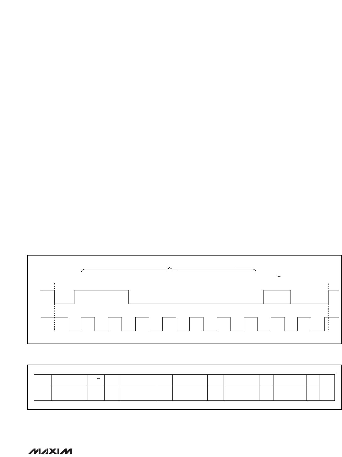
Read Cycle
There are only two registers on the MAX2160/EBG that
are available to be read by the master. When
addressed with a read command, the MAX2160/EBG
send back the contents of both read registers (STATUS
BYTE-1 and STATUS BYTE-2).
A read cycle begins with the bus master issuing a
START condition followed by the seven slave address
bits and a read bit (R/W = 1). If the slave address byte
is successfully received, the MAX2160/EBG issue an
ACK. The master then reads the contents of the STA-
TUS BYTE-1 register, beginning with the most signifi-
cant bit, and acknowledges if the byte is received
successfully. Next, the master reads the contents of the
STATUS BYTE-2 register. At this point the master can
issue an ACK or NACK and then a STOP condition to
terminate the read cycle.
Figure 3 illustrates an example in which the read regis-
ters are read by the master.
Applications Information
RF Input (RFIN)
The MAX2160/EBG are internally matched to 50Ω and
requires a DC-blocking capacitor (see the Typical
Operating Circuit).
RF Gain Control (GC1)
The MAX2160/EBG feature a variable-gain low-noise
amplifier that provides 43dB of RF gain-control range.
The voltage control (V
GC1
) range is 0.3V (minimum
attenuation) to 2.7V (maximum attenuation).
IF Power Detector
The MAX2160/EBG include a true RMS power detector
at the mixer output. The power-detector circuit is
enabled or disabled with the EPD bit in the control reg-
ister. The attack point can be set through the PD[2:0]
bits in the control register (see Table 5 for a summary
of attack point settings).
The PWRDET pin output can be configured to provide
either a voltage output (directly from the RMS power-
detector stage) or current output (default) through the
diagnostic bits D[2:0] in the test register.
Closed-Loop RF Power Control
The default mode of the IF power detector is current out-
put mode. Closed-loop RF power control is formed by
connecting the PWRDET pin directly to the GC1 pin. A
shunt capacitor to ground is added to set the closed-
loop response time (see the Typical Operating Circuit).
The recommended capacitor value of 10nF provides a
response time of 0.1ms.
Closed-loop RF power control can also be formed using
the baseband processor and the power detector in volt-
age output mode. In this configuration, the processor
senses the power detector’s output voltage and uses this
information to drive the GC1 pin directly. Voltage output
mode is enabled by setting the D[2:0] bits in the test reg-
ister to 100. In voltage mode, the PWRDET pin outputs a
scaled DC voltage proportional to the RF input power.
For the RF input range of -62dBm to -48dBm, the DC
output voltage ranges from 84mV to 420mV.
High-Side and Low-Side LO Injection
The MAX2160/EBG allow selection between high-side
and low-side LO injection through the HSLS bit in the
control register. High-side injection is the default setting
(HSLS = 1).
Q-Channel Shutdown
The Q channel low-IF output of the MAX2160/EBG can
be turned off with the QOFF bit in the XTAL divide reg-
ister for use with single low-IF input demodulators (use I
channel only). Turning off the Q channel reduces the
supply current by approximately 3mA.