MAX2160/MAX2160EBG
ISDB-T Single-Segment Low-IF Tuners
______________________________________________________________________________________ 19
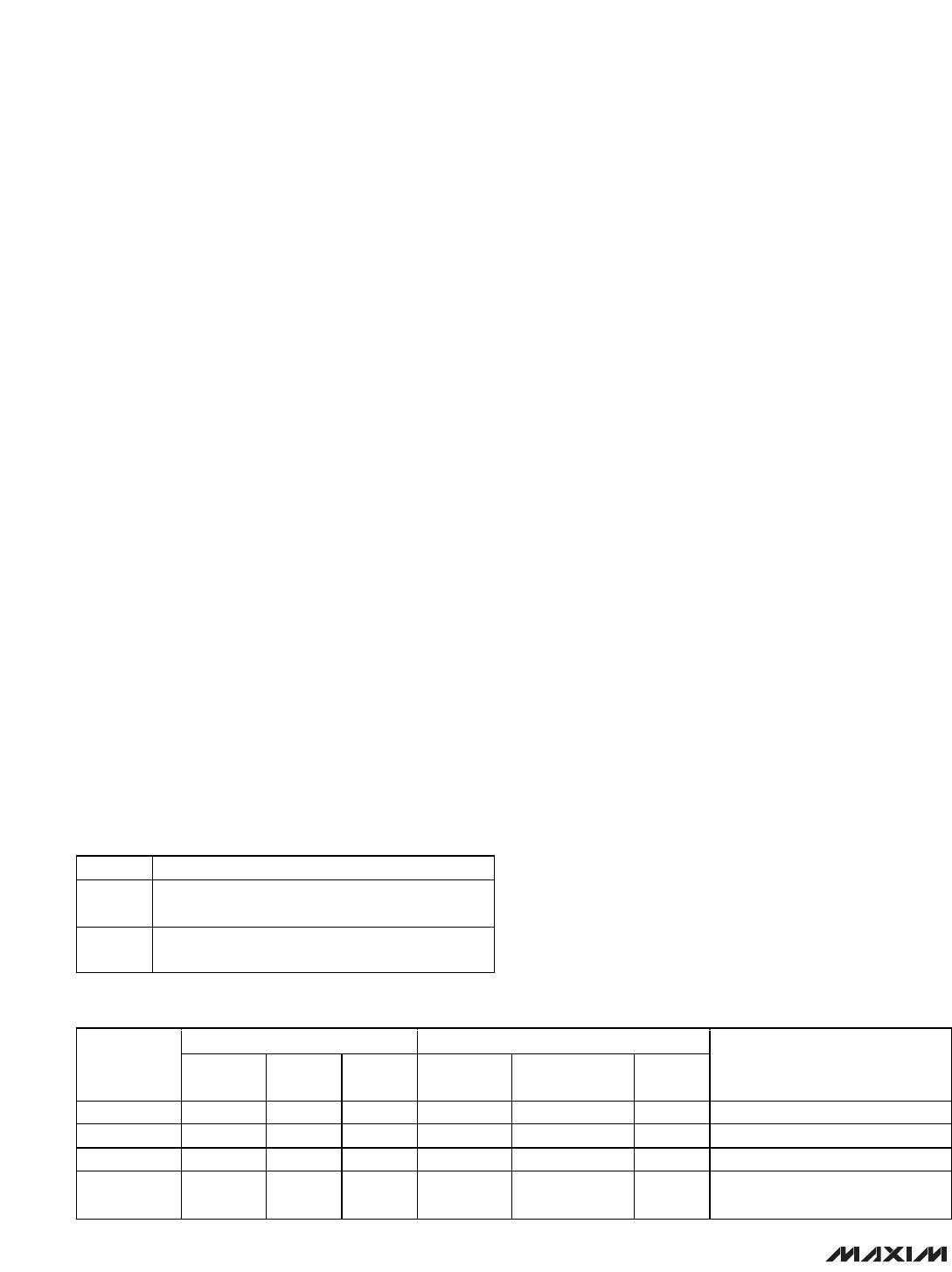
IF Filter Tuning
The center frequency of the baseband bandpass filter
is tuned to 571kHz during production at the factory.
However, the factory-set trim may be bypassed and the
filter’s center frequency can be adjusted through the
FLTS and TUN[2:0] bits in the test register. Setting the
FLTS bit sets the filter’s center frequency to the factory-
set tuning, clearing the FLTS bit allows the filter’s center
frequency to be adjusted with the TUN[2:0] bits (see
Table 2).
Fixed IF Gain Step
To maintain the best possible sensitivity for both QPSK
and QAM signals, the MAX2160/EBG include a control
bit (MOD) to increase the gain of the baseband stage
by approximately 7dB. This gain step is intended to be
used when receiving QPSK signals. Set the MOD bit to
one in QPSK receive mode, set the MOD bit to zero in
QAM receive mode.
VCO Autoselect (VAS)
The MAX2160/EBG include four VCOs with each VCO
having eight sub-bands. The local oscillator frequency
can be manually selected by programming the
VCO[1:0] and VSB[2:0] bits in the VCO register. The
selected VCO and sub-band is reported in the STATUS
BYTE-2 register (see Table 11).
Alternatively, the MAX2160/EBG can be set to automati-
cally choose a VCO and VCO sub-band. Automatic
VCO selection is enabled by setting the VAS bit in the
PLL register, and is initiated once the N-divider LSB
register word is loaded. In the event that only the R-
divider register or N-divider MSB register word is
changed, the N-divider LSB word must also be loaded
(last) to initiate the VCO autoselect function. The VCO
and VCO sub-band that are programmed in the
VCO[1:0] and VSB[2:0] bits serve as the starting point
for the automatic VCO selection process.
During the selection process, the VASE bit in the
STATUS BYTE-2 register is cleared to indicate the auto-
matic selection function is active. Upon successful
completion, bits VASE and VASA are set and the VCO
and sub-band selected are reported in the STATUS
BYTE-2 register (see Table 11). If the search is unsuc-
cessful, VASA is cleared and VASE is set. This indi-
cates that searching has ended but no good VCO has
been found, and occurs when trying to tune to a fre-
quency outside the VCO’s specified frequency range.
Charge-Pump Select (CPS)
The MAX2160/EBG also allow for manual selection of the
charge-pump current (CPS = 0) or automatic selection
based on the final VTUNE ADC read value (CPS = 1).
When in manual mode, the charge-pump current is pro-
grammed by bits CP[1:0] with the 2-wire bus. When in
automatic selection mode, the CP[1:0] bits are automati-
cally set according to the ADC table (see Tables 12 and
13). The selected charge-pump current (manually or
automatically) is reported in the STATUS BYTE-1 register.
3-Bit ADC
The MAX2160/EBG have an internal 3-bit ADC connect-
ed to the VCO tune pin (VTUNE). This ADC can be
used for checking the lock status of the VCOs.
Table 13 summarizes the ADC trip points, associated
charge-pump settings (when CPS = 1), and the VCO
lock indication. The VCO autoselect routine will only
select a VCO in the “VAS locked” range. This allows
room for a VCO to drift over temperature and remain in
a valid “locked” range.
The ADC must first be enabled by setting the ADE bit in
the VCO register. The ADC reading is latched by a sub-
sequent programming of the ADC latch bit (ADL = 1).
The ADC value is reported in the STATUS BYTE-2
register (see Table 11).
Table 12. Charge-Pump Current Selection