CYRF89135
Document Number: 001-86331 Rev. ** Page 10 of 41
Pinouts
The CYRF89135-68LTXC PRoC-EMB device is available in a 68-pin QFN package, which is illustrated in the following table. Every
port pin (labeled with a ā€œPā€) is capable of Digital I/O and connection to the common analog bus. However, V
DD
, and XRES are not
capable of Digital I/O.
Figure 4. 68-pin QFN pinout
Pin Definitions
This table gives the pin definitions.
[1, 2]
Pin No. Pin Name Description
1 TEST2 Reserved for factory test. Do not connect.
2 TEST3 Reserved for factory test. Do not connect.
3 VDD Core power supply voltage. Connect all VDD pins to VOUT pin
4 P0[4] Analog I/O, Digital I/O, VREF
5 P0[6] Analog I/O, Digital I/O
6 VIN Unregulated input voltage to the on-chip low drop out (LDO) voltage regulator.
7 VDD Core power supply voltage. Connect all VDD pins to VOUT pin.
8 OCDO OCD odd data IO, NC
9 OCDE OCD even data output, NC
10 P0[7] Analog I/O, Digital I/O,SPI CLK
11 P0[5] Analog I/O, Digital I/O
TEST2
TEST3
VDD
P0[4]
P0[6]
VIN
VDD
OCDO
OCDE
P0[7]
P0[5]
P0[3]
FIFO
P0[1]
VIN
OCDOE
P2[7]
P2[5]
PKT
RST_N
P2[3]
P2[1]
P4[1]
P3[7]
SPI_SS
P3[5]
P3[3]
P3[1]
CLK
MOSI
MISO
P1[7]
P1[5]
VDD
P1[6]
VDD
P1[4]
P1[2]
P1[0]
TEST1
NC
XTALI
XTALO
VDD
GND
P1[1]
VOUT
P1[3]
VIN
HCLK
CCLK
P0[2]
P0[0]
P2[6]
P2[4]
P2[2]
P2[0]
VDD
P4[2]
ANT
P4[0]
P3[6]
ANTB
P3[4]
P3[2]
P3[0]
VDD
XRES
51
50
49
48
47
46
45
44
43
42
41
40
39
38
37
36
35
68
67
66
65
64
63
62
61
60
59
58
57
56
55
54
53
52
10
11
12
13
14
15
16
17
1
2
3
4
5
6
7
8
9
18
19
20
21
22
23
24
25
26
27
28
29
30
31
32
33
34
CYRF89135 68-PIN QFN
Notes
1. Connect all VDD pin to VOUT pin.
2. Each of the ANT and ANTB pins much be DC grounded, 20 kļ— or less.
CYRF89135
Document Number: 001-86331 Rev. ** Page 11 of 41
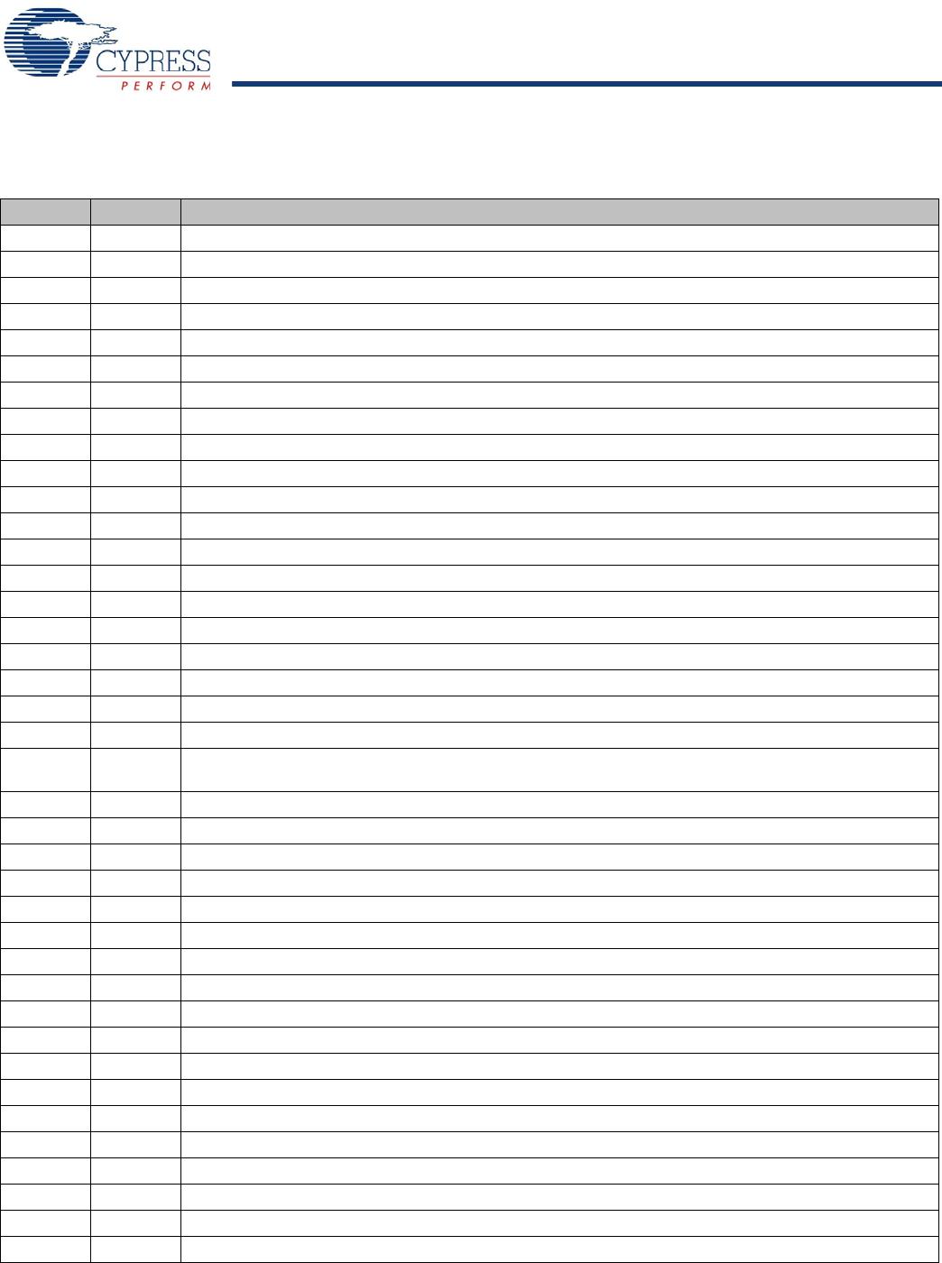
12 P0[3] Analog I/O, Digital I/O, Integrating input
13 FIFO FIFO status indicator bit
14 P0[1] Analog I/O, Digital I/O, Integrating input
15 VIN Unregulated input voltage to the on-chip low drop out (LDO) voltage regulator.
16 OCDOE OCD mode direction pin, NC
17 P2[7] Analog I/O, Digital I/O
18 P2[5] Analog I/O, Digital I/O, XTAL Out
19 P2[3] Analog I/O, Digital I/O, XTAL In
20 P2[1] Analog I/O, Digital I/O
21 P4[1] Analog I/O, Digital I/O
22 P3[7] Analog I/O, Digital I/O
23 SPI_SS Enable input for SPI, active low. Also used to bring device out of sleep state.
24 P3[5] Analog I/O, Digital I/O
25 P3[3] Analog I/O, Digital I/O
26 PKT Transmit/receive packet status indicator bit
27 P3[1] Analog I/O, Digital I/O
28 CLK Clock input for SPI interface
29 MOSI Data input for the SPI bus
30 MISO Data output (tristate when not active)
31 P1[7] Digital I/O, Analog I/O, I2C SCL, SPI SS
32 RST_N RST_N Low: Chip shutdown to conserve power. Register values lost
RST_N High: Turn on chip, registers restored to default value
33 P1[5] Digital I/O, Analog I/O, I2C SDA, SPI MISO
34 VDD Core power supply voltage. Connect all VDD pins to VOUT pin.
35 CCLK OCD CPU CLK OUTPUT, NC
36 HCLK OCD HIGH SPEED CLK, NC
37 VIN Unregulated input voltage to the on-chip low drop out (LDO) voltage regulator
38 P1[3] Digital I/O, Analog I/O, SPI CLK
39 VOUT 1.8 V output from on-chip LDO. Connect to all Vdd pins, do not connect to external loads.
40 P1[1] Digital I/O, Analog I/O, TC CLK, I2C SCL, SPI MOSI
41 GND Ground Pin
42 VDD Core power supply voltage. Connect all VDD pins to VOUT pin.
43 XTALO Output of the crystal oscillator gain block
44 XTALI Input to the crystal oscillator gain block
45 NC No Connect
46 TEST1 Reserved for factory test. Do not connect.
47 P1[0] Analog I/O, Digital I/O, TC DATA, I2C SDA
48 P1[2] Analog I/O, Digital I/O
49 P1[4] Analog I/O, Digital I/O, EXT CLK
50 VDD Core power supply voltage. Connect all VDD pins to VOUT pin.
Pin Definitions (continued)
This table gives the pin definitions.
[1, 2]
Pin No. Pin Name Description
CYRF89135
Document Number: 001-86331 Rev. ** Page 12 of 41
51 P1[6] Analog I/O, Digital I/O
52 XRES Active high external reset with internal pull down
53 VDD Core power supply voltage. Connect all VDD pins to VOUT pin.
54 P3[0] Analog I/O, Digital I/O
55 P3[2] Analog I/O, Digital I/O
56 P3[4] Analog I/O, Digital I/O.
57 ANTb Differential RF input/output.
58 P3[6] Analog I/O, Digital I/O.
59 P4[0] Analog I/O, Digital I/O.
60 ANT Differential RF input/output.
61 P4[2] Analog I/O, Digital I/O.
62 VDD Core power supply voltage. Connect all VDD pins to VOUT pin.
63 P2[0] Analog I/O, Digital I/O
64 P2[2] Analog I/O, Digital I/O
65 P2[4] Analog I/O, Digital I/O
66 P2[6] Analog I/O, Digital I/O
67 P0[0] Analog I/O, Digital I/O
68 P0[2] Analog I/O, Digital I/O
Pin Definitions (continued)
This table gives the pin definitions.
[1, 2]
Pin No. Pin Name Description

CYRF89135-68LTXC

Mfr. #:
Manufacturer:
Cypress Semiconductor
Description:
RF Transceiver Wireless Capacitive Touch
Lifecycle:
New from this manufacturer.
Delivery:
DHL FedEx Ups TNT EMS
Payment:
T/T Paypal Visa MoneyGram Western Union

Products related to this Datasheet