Document Number: 001-86331 Rev. ** Page 5 of 41
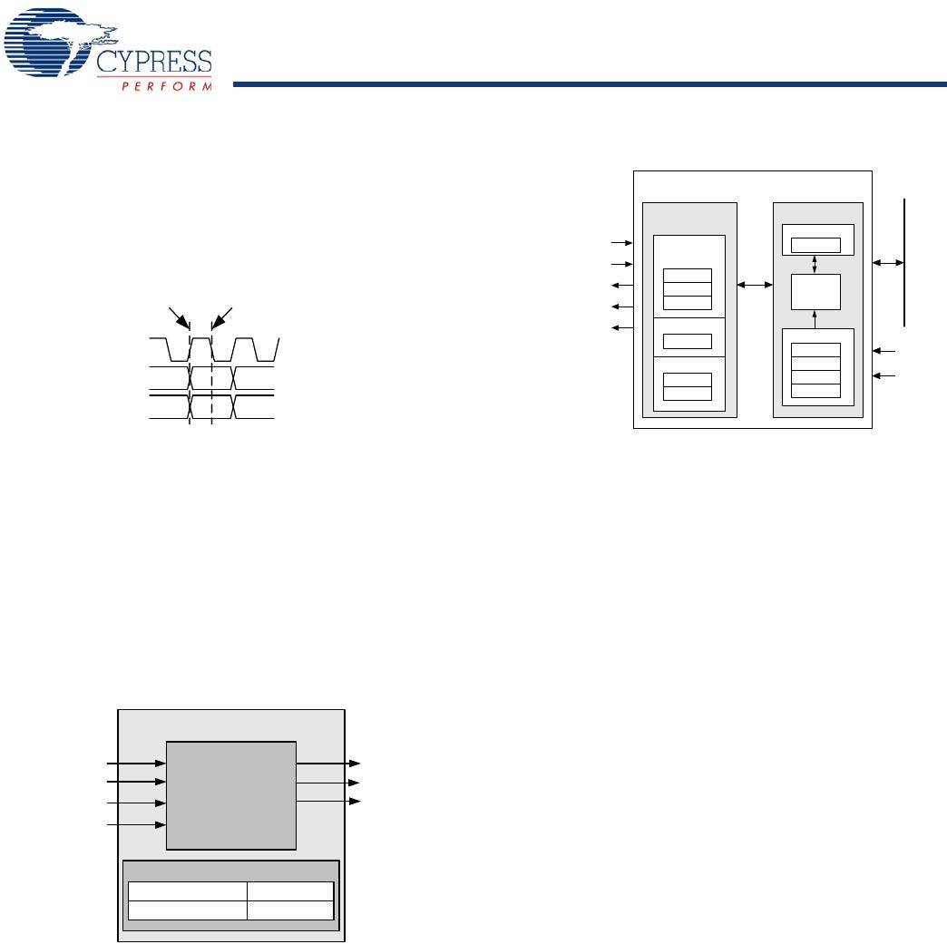
SPI
The serial peripheral interconnect (SPI) 3-wire protocol uses
both edges of the clock to enable synchronous communication
without the need for stringent setup and hold requirements.
Figure 1. Basic SPI Configuration
A device can be a master or slave. A master outputs clock and
data to the slave device and inputs slave data. A slave device
inputs clock and data from the master device and outputs data
for input to the master. Together, the master and slave are
essentially a circular Shift register, where the master generates
the clocking and initiates data transfers.
A basic data transfer occurs when the master sends eight bits of
data, along with eight clocks. In any transfer, both master and
slave transmit and receive simultaneously. If the master only
sends data, the received data from the slave is ignored. If the
master wishes to receive data from the slave, the master must
send dummy bytes to generate the clocking for the slave to send
data back.
I
2
C Slave
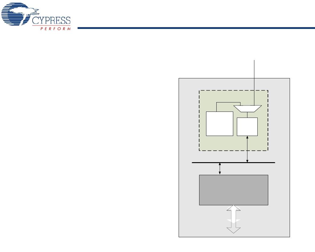
The I
2
C slave enhanced communications block is a
serial-to-parallel processor, designed to interface the
PRoC-EMB device to a two-wire I
2
C serial communications bus.
To eliminate the need for excessive CPU intervention and
overhead, the block provides I
2
C-specific support for status
detection and generation of framing bits. By default, the I
2
C
Slave Enhanced module is firmware compatible with the
previous generation of I
2
C slave functionality. However, this
module provides new features that are configurable to
implement significant flexibility for both internal and external
interfacing.
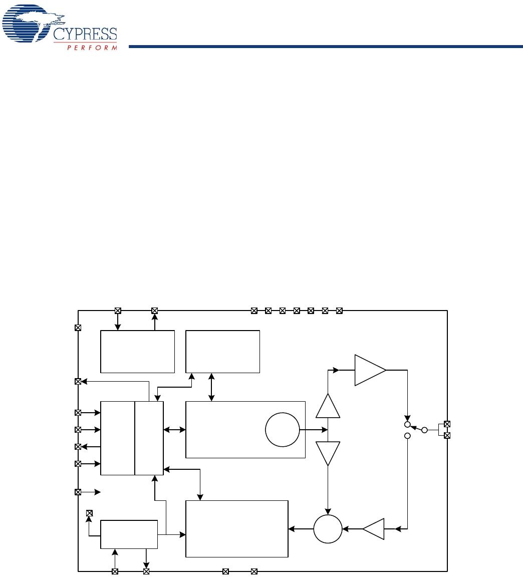
Figure 2. I
2
C Block Diagram
The basic I2C features include
■ Slave, transmitter, and receiver operation
■ Byte processing for low CPU overhead
■ Interrupt or polling CPU interface
■ Support for clock rates of up to 400 kHz
■ 7- or 10-bit addressing (through firmware support)
■ SMBus operation (through firmware support)
Enhanced features of the I
2
C Slave Enhanced Module include:
■ Support for 7-bit hardware address compare
■ Flexible data buffering schemes
■ A ‘no bus stalling’ operating mode
A low power bus monitoring modeThe I
2
C block controls the data
(SDA) and the clock (SCL) to the external I
2
C interface through
direct connections to two dedicated GPIO pins. When I
2
C is
enabled, these GPIO pins are not available for general purpose
use. The enCoRe V LV CPU firmware interacts with the block
through I/O register reads and writes, and firmware
synchronization is implemented through polling and/or
interrupts.
WirelessUSB NL System
WirelessUSB NL, optimized to operate in the 2.4-GHz ISM band,
is Cypress's third generation of 2.4-GHz low-power RF
technology. WirelessUSB NL implements a Gaussian
frequency-shift keying (GFSK) radio using a differentiated
single-mixer, closed-loop modulation design that optimizes
power efficiency and interference immunity. Closed-loop
modulation effectively eliminates the problem of frequency drift,
enabling WirelessUSB NL to transmit up to 255-byte payloads
without repeatedly having to pay power penalties for re-locking
the phase-locked loop (PLL) as in open-loop designs
Among the advantages of WirelessUSB NL are its fast lock times
and channel switching, along with the ability to transmit larger
payloads. Use of longer payload packets, compared to multiple
short payload packets, can reduce overhead, improve overall
power efficiency, and help alleviate spectrum crowding.
MOSI
MISO
SCLK
Data is output by
both the Master
and Slave on
one edge of the
clock.
Data is registered at the
input of both devices on the
opposite edge of the clock.
SPI Block
Registers
SYSCLK
DATA_OUTDATA_IN
CLK_IN CLK_OUT
INT
SS_
SCLK
MOSI,
MISO
SCLK
MOSI,
MISO
CONFIGURATION[7:0] CONTROL[7:0]
TRANSMIT[7:0] RECEIVE[7:0]
I2C Core
I2C Basic
Configuration
I2C_CFG
I2C_SCR
I2C_DR
Plus Features
HW Addr Cmp
Buffer Module
CPU Port
Buffer Ctl
32 Byte RAM
I2C Plus
Slave
I2C_ADDR
SDA_OUT
SCL_IN
SYSCLK
I2C_EN
To/From
GPIO
Pins
STANDBY
SCL_OUT
SDA_IN
I2C_XSTAT
I2C_XCFG
I2C_BUF
I2C_BP
I2C_CP
MCU_CP
MCU_BP
System Bus