Document Number: 001-86331 Rev. ** Page 20 of 41
DC POR and LVD Specifications
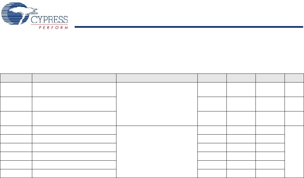
The following table lists guaranteed maximum and minimum specifications for the entire voltage and temperature ranges.
Table 11. DC POR and LVD Specifications
Symbol Description Conditions Min Typ Max Units
V
POR1
2.36 V selected in PSoC Designer
PORLEV[1:0] = 00b, HPOR = 1
V
IN
must be greater than or equal
to 1.9 V during startup, reset from
the XRES pin, or reset from
watchdog.
–2.362.41V
V
POR2
2.60 V selected in PSoC Designer
PORLEV[1:0] = 01b, HPOR = 1
–2.602.66
V
POR3
2.82 V selected in PSoC Designer
PORLEV[1:0] = 10b, HPOR = 1
–2.822.95
V
LVD0
2.45 V selected in PSoC Designer – 2.40 2.45 2.51 V
V
LVD1
2.71 V selected in PSoC Designer 2.64
[8]
2.71 2.78
V
LVD2
2.92 V selected in PSoC Designer 2.85
[9]
2.92 2.99
V
LVD3
3.02 V selected in PSoC Designer 2.95
[10]
3.02 3.09
V
LVD4
3.13 V selected in PSoC Designer 3.06 3.13 3.20
V
LVD5
1.90 V selected in PSoC Designer 1.84 1.90 2.32
Notes
8. Always greater than 50 mV above V
PPOR1
voltage for falling supply.
9. Always greater than 50 mV above V
PPOR2
voltage for falling supply.
10. Always greater than 50 mV above V
PPOR3
voltage for falling supply.

