Document Number: 001-86331 Rev. ** Page 23 of 41
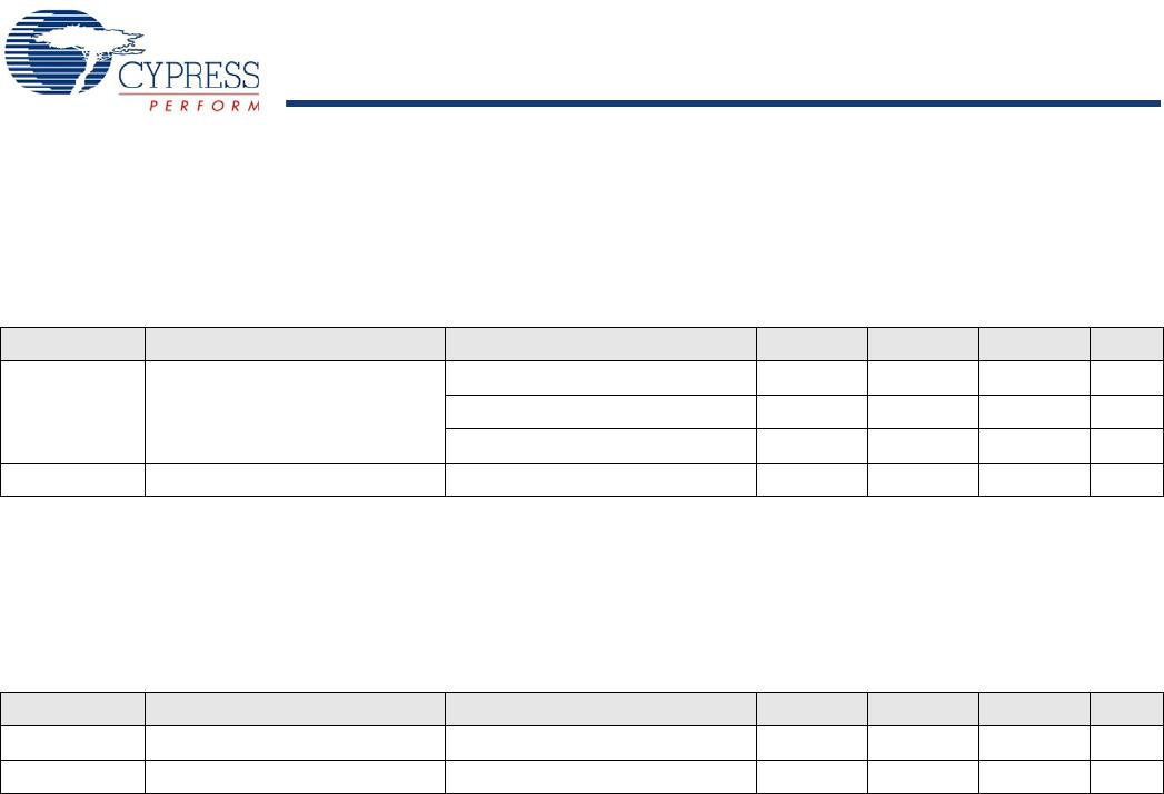
AC Chip-Level Specifications
The following table lists guaranteed maximum and minimum specifications for the entire voltage and temperature ranges.
Table 15. AC Chip-Level Specifications
Symbol Description Conditions Min Typ Max Units
F
IMO24
IMO frequency at
24 MHz Setting
– 22.8 24 25.2 MHz
F
IMO12
IMO frequency at 12 MHz setting – 11.4 12 12.6 MHz
F
IMO6
IMO frequency at 6 MHz setting – 5.7 6.0 6.3 MHz
F
CPU
CPU frequency – 0.75 – 25.20 MHz
F
32K1
ILO frequency – 19 32 50 kHz
F
32K_U
ILO untrimmed frequency – 13 32 82 kHz
DC
IMO
Duty cycle of IMO – 40 50 60 %
DC
ILO
ILO duty cycle – 40 50 60 %
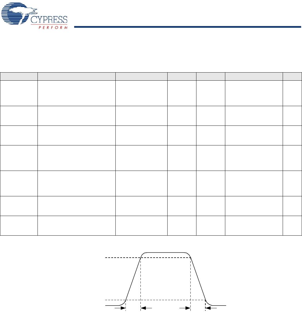
SR
POWER_UP
Power supply slew rate VIN slew rate during power-up – – 250 V/ms
t
XRST
External reset pulse width at
power-up
After supply voltage is valid 1 – – ms
t
XRST2
External reset pulse width after
power-up
Applies after part has booted 10 – – s
t
OS
Startup time of ECO – – 1 – s
t
JIT_IMO
N = 32 6 MHz IMO cycle-to-cycle jitter
(RMS)
– 0.7 6.7 ns
6 MHz IMO long term N (N = 32)
cycle-to-cycle jitter (RMS)
– 4.3 29.3 ns
6 MHz IMO period jitter (RMS) – 0.7 3.3 ns
12 MHz IMO cycle-to-cycle jitter
(RMS)
– 0.5 5.2 ns
12 MHz IMO long term N (N = 32)
cycle-to-cycle jitter (RMS)
– 2.3 5.6 ns
12 MHz IMO period jitter (RMS) – 0.4 2.6 ns
24 MHz IMO cycle-to-cycle jitter
(RMS)
– 1.0 8.7 ns
24 MHz IMO long term N (N = 32)
cycle-to-cycle jitter (RMS)
– 1.4 6.0 ns
24 MHz IMO period jitter (RMS) – 0.6 4.0 ns