10
FN8165.3
August 29, 2006
Transfer Wiper Counter Register (WCR) to Data Register (DR)
Increment/Decrement Wiper Counter Register (WCR)
Global Transfer Data Register (DR) to Wiper Counter Register (WCR)
Global Transfer Wiper Counter Register (WCR) to Data Register (DR)
Read Status
CS
Falling
Edge
device type
identifier
device
addresses
instruction
opcode
DR and WCR
addresses
CS
Rising
Edge
HIGH-VOLTAGE
WRITE CYCLE
010100
A
1
A
0
1110
R
1
R
0
P
1
P
0
CS
Falling
Edge
device type
identifier
device
addresses
instruction
opcode
WCR
addresses
increment/decrement
(sent by master on SI)
CS
Rising
Edge
010100
A
1
A
0
0010XX
P
1
P
0
I/D I/D . . . . I/D I/D
CS
Falling
Edge
device type
identifier
device
addresses
instruction
opcode
DR
addresses
CS
Rising
Edge
010100
A
1
A
0
0001
R
1
R
0
00
CS
Falling
Edge
device type
identifier
device
addresses
instruction
opcode
DR
addresses
CS
Rising
Edge
HIGH-VOLTAGE
WRITE CYCLE
010100
A
1
A
0
1000
R
1
R
0
00
CS
Falling
Edge
device type
identifier
device
addresses
instruction
opcode
Data Byte
(sent by X9250 on SO)
CS
Rising
Edge
010100
A
1
A
0
010100010000000
W
I
P
X9250
11
FN8165.3
August 29, 2006
ABSOLUTE MAXIMUM RATINGS
Temperature under bias ........................ -65 to +135°C
Storage temperature ............................. -65 to +150°C
Voltage on SCK, SCL or any address input
with respect to V
SS
................................. -1V to +7V
Voltage on V+ (referenced to V
SS
)........................ 10V
Voltage on V- (referenced to V
SS
)........................-10V
(V+) - (V-) .............................................................. 12V
Any V
H
/R
H
..............................................................V+
Any V
L
/R
L
.................................................................V-
Lead temperature (soldering, 10s) .................. +300°C
I
W
(10s) ............................................................±15mA
COMMENT
Stresses above those listed under “Absolute Maximum
Ratings” may cause permanent damage to the device.
This is a stress rating only; functional operation of the
device (at these or any other conditions above those
listed in the operational sections of this specification) is
not implied. Exposure to absolute maximum rating
conditions for extended periods may affect device
reliability.
POTENTIOMETER CHARACTERISTICS
(Over recommended operating conditions unless otherwise stated.)
Notes: (1) Absolute linearity is utilized to determine actual wiper voltage versus expected voltage as determined by wiper position when used as a
potentiometer.
(2) Relative linearity is utilized to determine the actual change in voltage between two successive tap positions when used as a potentiom-
eter. It is a measure of the error in step size.
(3) MI = RTOT/255 or (V
H
/R
H
- V
L
/R
L
)/255, single pot
(4) Individual array resolutions.
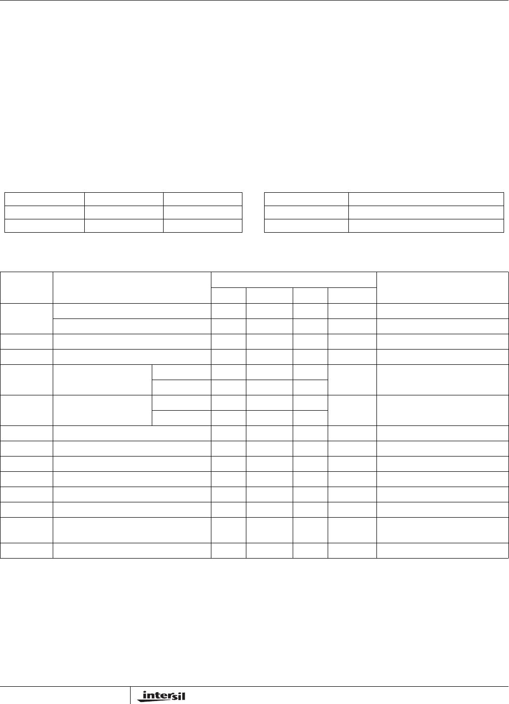
Symbol Parameter
Limits
Test ConditionsMin. Typ. Max. Unit
End to end resistance tolerance ±20 %
Power rating 50 mW +25°C, each pot
I
W
Wiper current ±7.5 mA
R
W
Wiper resistance 150 250 Wiper current = ± 1mA
Vv+ Voltage on V+ pin X9250 +4.5 +5.5 V
X9250-2.7 +2.7 +5.5
Vv- Voltage on V- pin X9250 -5.5 -4.5 V
X9250-2.7 -5.5 -2.7
V
TERM
Voltage on any V
H
/R
H
or V
L
/R
L
pin V- V+ V
Noise -120 dBV Ref: 1kHz
Resolution
(4)
0.6 %
Absolute linearity
(1)
±1 MI
(3)
V
w(n)(actual)
- V
w(n)(expected)
Relative linearity
(2)
±0.6 MI
(3)
V
w(n + 1 -
[V
w(n) + MI
]
Temperature coefficient of R
TOTAL
±300 ppm/°C
Ratiometric Temperature
Coefficient
±20 ppm/°C
C
H
/C
L
/C
W
Potentiometer Capacitances 10/10/25 pF See Circuit #3
RECOMMENDED OPERATING CONDITIONS
Temp Min. Max.
Commercial 0°C+70°C
Industrial -40°C+85°C
Device Supply Voltage (V
CC
) Limits
(4)
X9250 5V ±10%
X9250-2.7 2.7V to 5.5V
X9250
12
FN8165.3
August 29, 2006
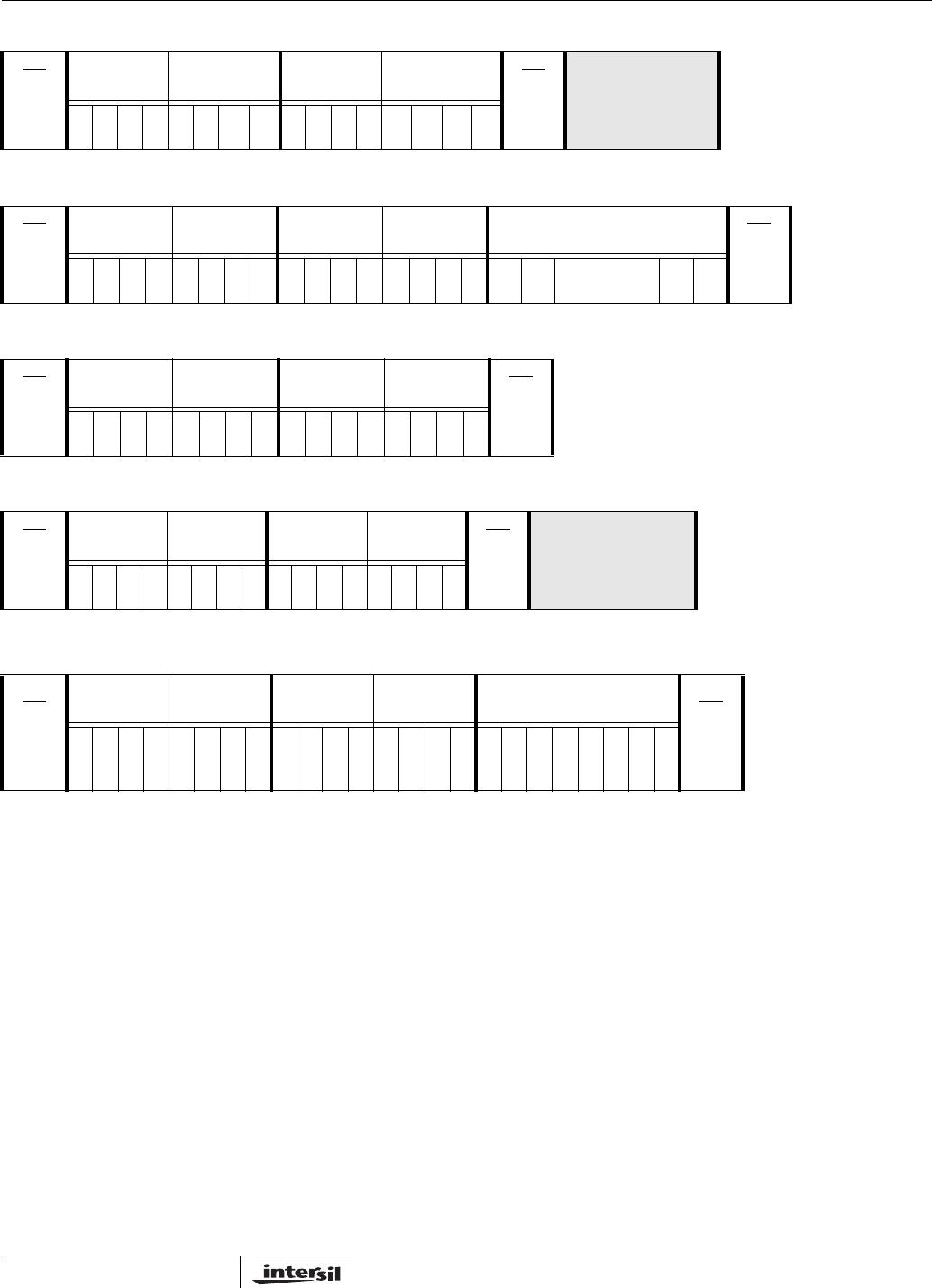
D.C. OPERATING CHARACTERISTICS (Over the recommended operating conditions unless otherwise specified.)
ENDURANCE AND DATA RETENTION
CAPACITANCE
POWER-UP TIMING
POWER UP AND DOWN REQUIREMENT
The are no restrictions on the sequencing of the bias supplies V
CC
, V+, and V- provided that all three supplies reach
their final values within 1msec of each other. At all times, the voltages on the potentiometer pins must be less than V+
and more than V-. The recall of the wiper position from nonvolatile memory is not in effect until all supplies reach their
final value. The V
CC
ramp rate spec is always in effect.
Notes: (5) This parameter is periodically sampled and not 100% tested
(6) t
PUR
and t
PUW
are the delays required from the time the third (last) power supply (V
CC
, V+ or V-) is stable until the specific instruction can be
issued. These parameters are periodically sampled and not 100% tested.
(7) Sample tested only.
A.C. TEST CONDITIONS
Symbol Parameter
Limits
Test ConditionsMin. Typ. Max. Unit
I
CC1
V
CC
supply current
(active)
400 µA f
SCK
= 2MHz, SO = Open,
Other Inputs = V
SS
I
CC2
V
CC
supply current
(nonvolatile write)
1mAf
SCK
= 2MHz, SO = Open,
Other Inputs = V
SS
I
SB
V
CC
current (standby) 5 µA SCK = SI = V
SS
, Addr. = V
SS
I
LI
Input leakage current 10 µA V
IN
= V
SS
to V
CC
I
LO
Output leakage current 10 µA V
OUT
= V
SS
to V
CC
V
IH
Input HIGH voltage V
CC
x 0.7 V
CC
+ 0.1 V
V
IL
Input LOW voltage -0.5 V
CC
x 0.3 V
V
OL
Output LOW voltage 0.4 V I
OL
= 3mA
Parameter Min. Unit
Minimum endurance 100,000 Data changes per bit per register
Data retention 100 Years
Symbol Test Max. Unit Test Conditions
C
OUT
(5)
Output capacitance (SO) 8 pF V
OUT
= 0V
C
IN
(5)
Input capacitance (A0, A1, SI, and SCK, CS) 6 pF V
IN
= 0V
Symbol Parameter Min. Max. Unit
t
PUR
(6)
Power-up to initiation of read operation 1 ms
t
PUW
(6)
Power-up to initiation of write operation 5 ms
t
R
V
CC
(7)
V
CC
power up ramp rate 0.2 50 V/msec
Input pulse levels V
CC
x 0.1 to V
CC
x 0.9
Input rise and fall times 10ns
Input and output timing level V
CC
x 0.5
X9250

X9250US24Z-2.7

Mfr. #:
Manufacturer:
Renesas / Intersil
Description:
Digital Potentiometer ICs SPI XDCP 100K QD 256 TAPS
Lifecycle:
New from this manufacturer.
Delivery:
DHL FedEx Ups TNT EMS
Payment:
T/T Paypal Visa MoneyGram Western Union