4
FN8165.3
August 29, 2006
DEVICE DESCRIPTION
Serial Interface
The X9250 supports the SPI interface hardware
conventions. The device is accessed via the SI input
with data clocked in on the rising SCK. CS
must be
LOW and the HOLD
and WP pins must be HIGH
during the entire operation.
The SO and SI pins can be connected together, since
they have three state outputs. This can help to reduce
system pin count.
Array Description
The X9250 is comprised of four resistor arrays. Each
array contains 255 discrete resistive segments that
are connected in series. The physical ends of each
array are equivalent to the fixed terminals of a
mechanical potentiometer (V
H
/R
H
and V
L
/R
L
inputs).
At both ends of each array and between each resistor
segment is a CMOS switch connected to the wiper
(V
W
/R
W
) output. Within each individual array only one
switch may be turned on at a time.
These switches are controlled by a Wiper Counter
Register (WCR). The 8 bits of the WCR are decoded
to select, and enable, one of 256 switches.
Wiper Counter Register (WCR)
The X9250 contains four Wiper Counter Registers,
one for each XDCP potentiometer. The WCR is
equivalent to a serial-in, parallel-out register/counter
with its outputs decoded to select one of 256 switches
along its resistor array. The contents of the WCR can
be altered in four ways: it may be written directly by
the host via the write Wiper Counter Register
instruction (serial load); it may be written indirectly by
transferring the contents of one of four associated
Data Registers via the XFR Data Register or Global
XFR Data Register instructions (parallel load); it can
be modified one step at a time by the
increment/decrement instruction. Finally, it is loaded
with the contents of its Data Register zero (DR0) upon
power-up.
The Wiper Counter Register is a volatile register; that
is, its contents are lost when the X9250 is powered-
down. Although the register is automatically loaded
with the value in R0 upon power-up, this may be
different from the value present at power-down.
Data Registers
Each potentiometer has four 8-bit nonvolatile Data
Registers. These can be read or written directly by the
host. Data can also be transferred between any of the
four Data Registers and the associated Wiper Counter
Register. All operations changing data in one of the
Data Registers is a nonvolatile operation and will take
a maximum of 10ms.
If the application does not require storage of multiple
settings for the potentiometer, the Data Registers can
be used as regular memory locations for system
parameters or user preference data.
Data Register Detail
(MSB) (LSB)
D7 D6 D5 D4 D3 D2 D1 D0
NV NV NV NV NV NV NV NV
X9250
5
FN8165.3
August 29, 2006
Figure 1. Detailed Potentiometer Block Diagram
Write in Process
The contents of the Data Registers are saved to
nonvolatile memory when the CS
pin goes from LOW
to HIGH after a complete write sequence is received
by the device. The progress of this internal write
operation can be monitored by a write in process bit
(WIP). The WIP bit is read with a read status
command.
INSTRUCTIONS
Identification (ID) Byte
The first byte sent to the X9250 from the host,
following a CS
going HIGH to LOW, is called the
Identification byte. The most significant four bits of the
slave address are a device type identifier, for the
X9250 this is fixed as 0101[B] (refer to Figure 2).
The two least significant bits in the ID byte select one
of four devices on the bus. The physical device
address is defined by the state of the A
0
- A
1
input
pins. The X9250 compares the serial data stream with
the address input state; a successful compare of both
address bits is required for the X9250 to successfully
continue the command sequence. The A
0
- A
1
inputs
can be actively driven by CMOS input signals or tied to
V
CC
or V
SS
.
The remaining two bits in the slave byte must be set to 0.
Figure 2. Identification Byte Format
Instruction Byte
The next byte sent to the X9250 contains the
instruction and register pointer information. The four
most significant bits are the instruction. The next four
bits point to one of the four pots and, when applicable,
they point to one of four associated registers. The
format is shown below in Figure 3.
Figure 3. Instruction Byte Format
Serial Data Path
From Interface
Circuitry
Register 0 Register 1
Register 2 Register 3
Serial
Bus
Input
Parallel
Input
Counter
Register
Inc/Dec
Logic
UP/DN
CLK
Modified SCK
UP/DN
V
H
/R
H
V
L
/R
L
V
W
/R
W
88
C
o
u
n
t
e
r
D
e
c
o
d
e
If WCR = 00[H] then V
W
/R
W
= V
L
/R
L
If WCR = FF[H] then V
W
/R
W
= V
H
/R
H
Wiper
(One of Four Arrays)
(WCR)
Bus
100
0 0 A1 A0
Device Type
Identifier
Device Address
1
I1I2I3 I0 R1 R0 P1 P0
Pot Select
Register
Select
Instructions
X9250
6
FN8165.3
August 29, 2006
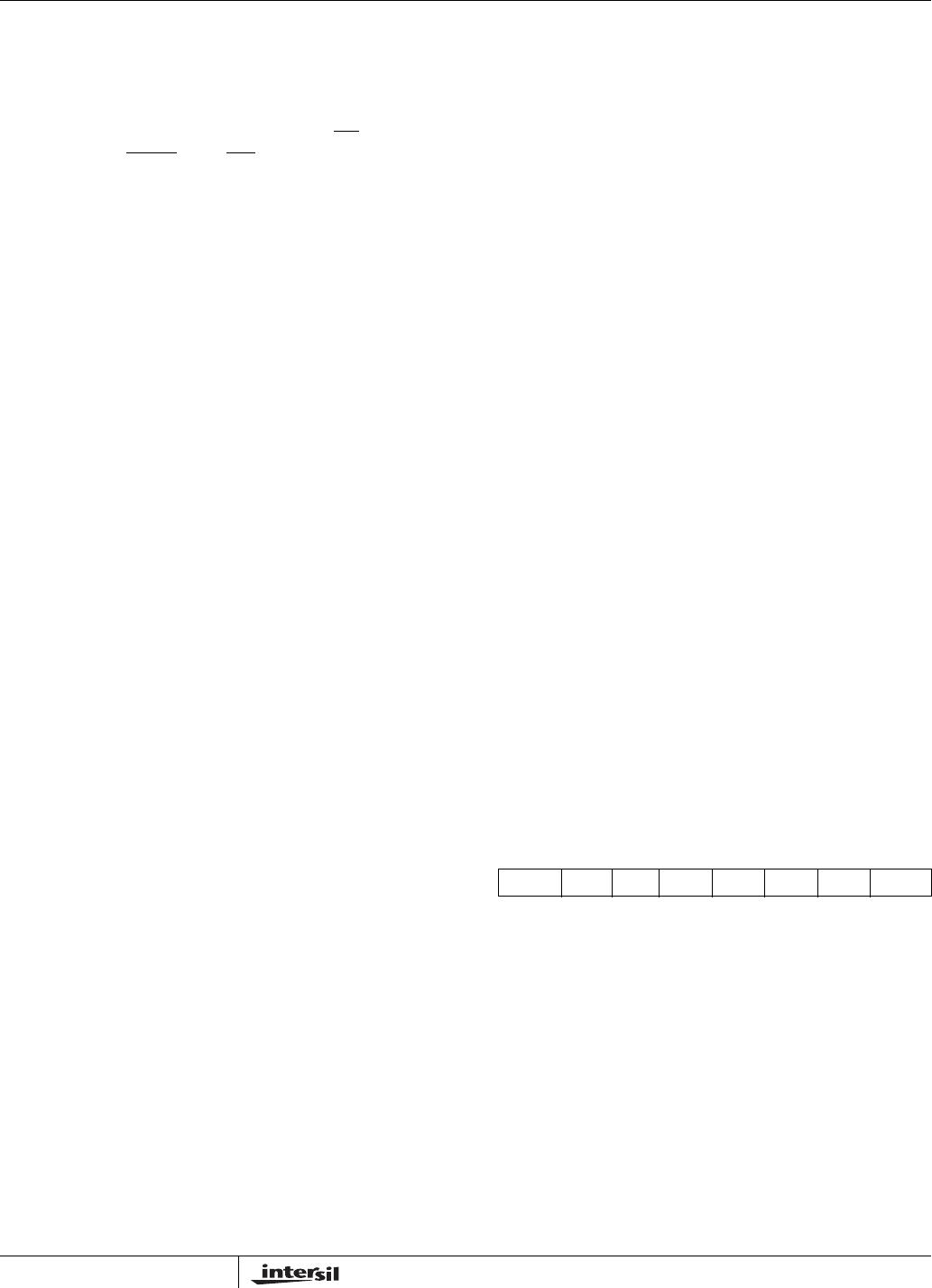
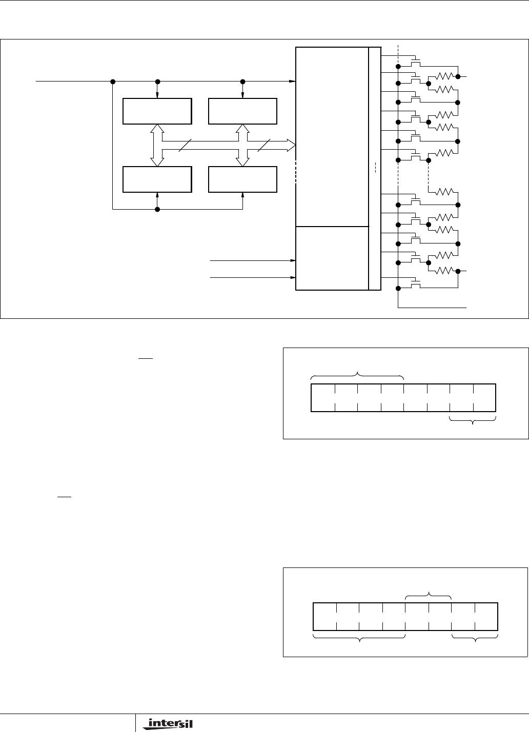
The four high order bits of the instruction byte specify
the operation. The next two bits (R
1
and R
0
) select
one of the four registers that is to be acted upon when
a register oriented instruction is issued. The last two
bits (P1 and P
0
) selects which one of the four
potentiometers is to be affected by the instruction.
Four of the ten instructions are two bytes in length and
end with the transmission of the instruction byte.
These instructions are:
XFR Data Register to Wiper Counter Register
—This
transfers the contents of one specified Data Register
to the associated Wiper Counter Register.
XFR Wiper Counter Register to Data Register
—This
transfers the contents of the specified Wiper
Counter Register to the specified associated Data
Register.
Global XFR Data Register to Wiper Counter Regiter
This transfers the contents of all specified Data Reg-
isters to the associated Wiper Counter Registers.
Global XFR Wiper Counter Register to Data Regiter
This transfers the contents of all Wiper Counter
Registers to the specified associated Data Regis-
ters.
The basic sequence of the two byte instructions is
illustrated in Figure 4. These two-byte instructions
exchange data between the WCR and one of the Data
Registers. A transfer from a Data Register to a WCR is
essentially a write to a static RAM, with the static RAM
controlling the wiper position. The response of the
wiper to this action will be delayed by t
WRL
. A transfer
from the WCR (current wiper position), to a Data
Register is a write to nonvolatile memory and takes a
minimum of t
WR
to complete. The transfer can occur
between one of the four potentiometers and one of its
associated registers; or it may occur globally, where
the transfer occurs between all potentiometers and one
associated register.
Five instructions require a three-byte sequence to
complete. These instructions transfer data between
the host and the X9250; either between the host and
one of the data registers or directly between the host
and the Wiper Counter Register. These instructions
are:
Read Wiper Counter Register
—read the current
wiper position of the selected pot,
Write Wiper Counter Register
—change current
wiper position of the selected pot,
Read Data Register
—read the contents of the
selected data register;
Write Data Register
—write a new value to the
selected data register.
Read Status
—This command returns the contents
of the WIP bit which indicates if the internal write
cycle is in progress.
The sequence of these operations is shown in Figure
5 and Figure 6.
The final command is Increment/Decrement. It is
different from the other commands, because it’s length
is indeterminate. Once the command is issued, the
master can clock the selected wiper up and/or down in
one resistor segment steps; thereby, providing a fine
tuning capability to the host. For each SCK clock pulse
(t
HIGH
) while SI is HIGH, the selected wiper will move
one resistor segment towards the V
H
/R
H
terminal.
Similarly, for each SCK clock pulse while SI is LOW,
the selected wiper will move one resistor segment
towards the V
L
/R
L
terminal. A detailed illustration of the
sequence and timing for this operation are shown in
Figure 7 and Figure 8.
X9250

X9250US24Z-2.7

Mfr. #:
Manufacturer:
Renesas / Intersil
Description:
Digital Potentiometer ICs SPI XDCP 100K QD 256 TAPS
Lifecycle:
New from this manufacturer.
Delivery:
DHL FedEx Ups TNT EMS
Payment:
T/T Paypal Visa MoneyGram Western Union