7
FN8165.3
August 29, 2006
Figure 4. Two-Byte Instruction Sequence
Figure 5. Three-Byte Instruction Sequence (Write)
Figure 6. Three-Byte Instruction Sequence (Read)
Figure 7. Increment/Decrement Instruction Sequence
010100A1A0 I3 I2 I1 I0 R1 R0 P1 P0
SCK
SI
CS
0 1 0 1 A1 A0 I3 I2 I1 I0 R1 R0 P1 P0
SCL
SI
D7 D6 D5 D4 D3 D2 D1 D0
CS
00
0 1 0 1 A1 A0 I3 I2 I1 I0 R1 R0 P1 P0
SCL
SI
CS
00
S0
D7 D6 D5 D4 D3 D2 D1 D0
Don’t Care
010100A1A0 I3 I2 I1 I0 0
P1
P0
SCK
SI
I
N
C
1
I
N
C
2
I
N
C
n
D
E
C
1
D
E
C
n
0
CS
X9250
8
FN8165.3
August 29, 2006
Figure 8. Increment/Decrement Timing Limits
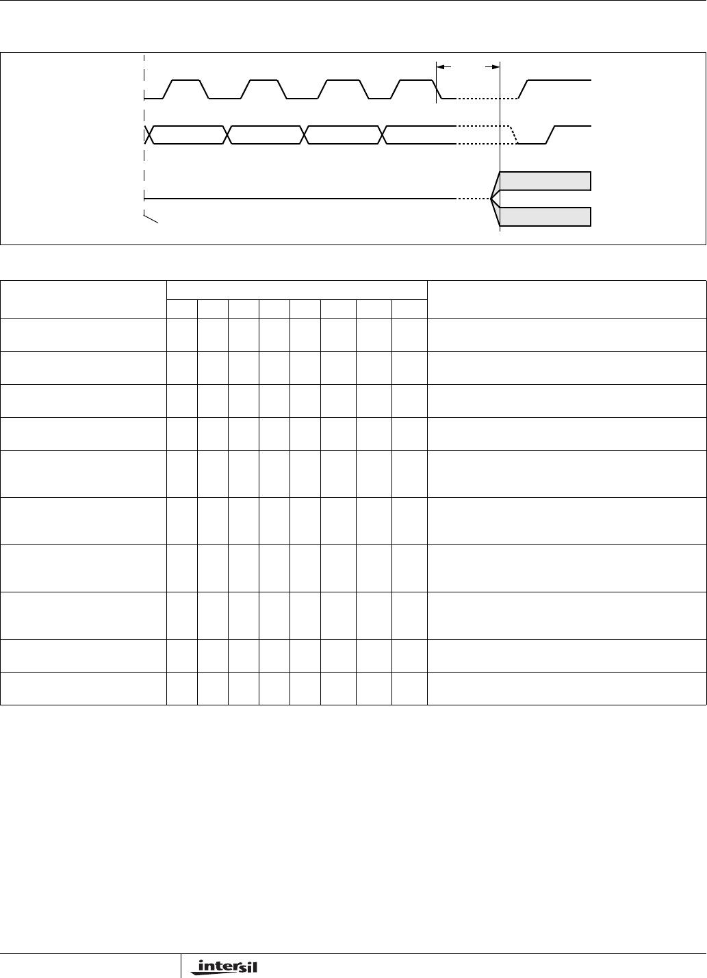
Table 1. Instruction Set
Instruction
Instruction Set
OperationI
3
I
2
I
1
I
0
R
1
R
0
P
1
P
0
Read Wiper Counter
Register
10010 0P
1
P
0
Read the contents of the Wiper Counter
Register pointed to by P
1
- P
0
Write Wiper Counter
Register
10100 0P
1
P
0
Write new value to the Wiper Counter Register
pointed to by P
1
- P
0
Read Data Register 1 0 1 1 R
1
R
0
P
1
P
0
Read the contents of the Data Register
pointed to by P
1
- P
0
and R
1
- R
0
Write Data Register 1 1 0 0 R
1
R
0
P
1
P
0
Write new value to the Data Register pointed to
by P
1
- P
0
and R
1
- R
0
XFR Data Register to
Wiper Counter Register
1101R
1
R
0
P
1
P
0
Transfer the contents of the Data Register
pointed to by R
1
- R
0
to the Wiper Counter
Register pointed to by P
1
- P
0
XFR Wiper Counter
Register to Data Register
1110R
1
R
0
P
1
P
0
Transfer the contents of the Wiper Counter
Register pointed to by P
1
- P
0
to the Register
pointed to by R
1
- R
0
Global XFR Data Register
to Wiper Counter Register
0001R
1
R
0
0 0 Transfer the contents of the Data Registers
pointed to by R
1
- R
0
of all four pots to their
respective Wiper Counter Register
Global XFR Wiper Counter
Register to Data Register
1000R
1
R
0
0 0 Transfer the contents of all Wiper Counter
Registers to their respective data Registers
pointed to by R
1
- R
0
of all four pots
Increment/Decrement
Wiper Counter Register
00100 0P
1
P
0
Enable Increment/decrement of the Wiper
Counter Register pointed to by P
1
- P
0
Read Status (WIP bit) 0 1010 0 0 1Read the status of the internal write cycle, by
checking the WIP bit.
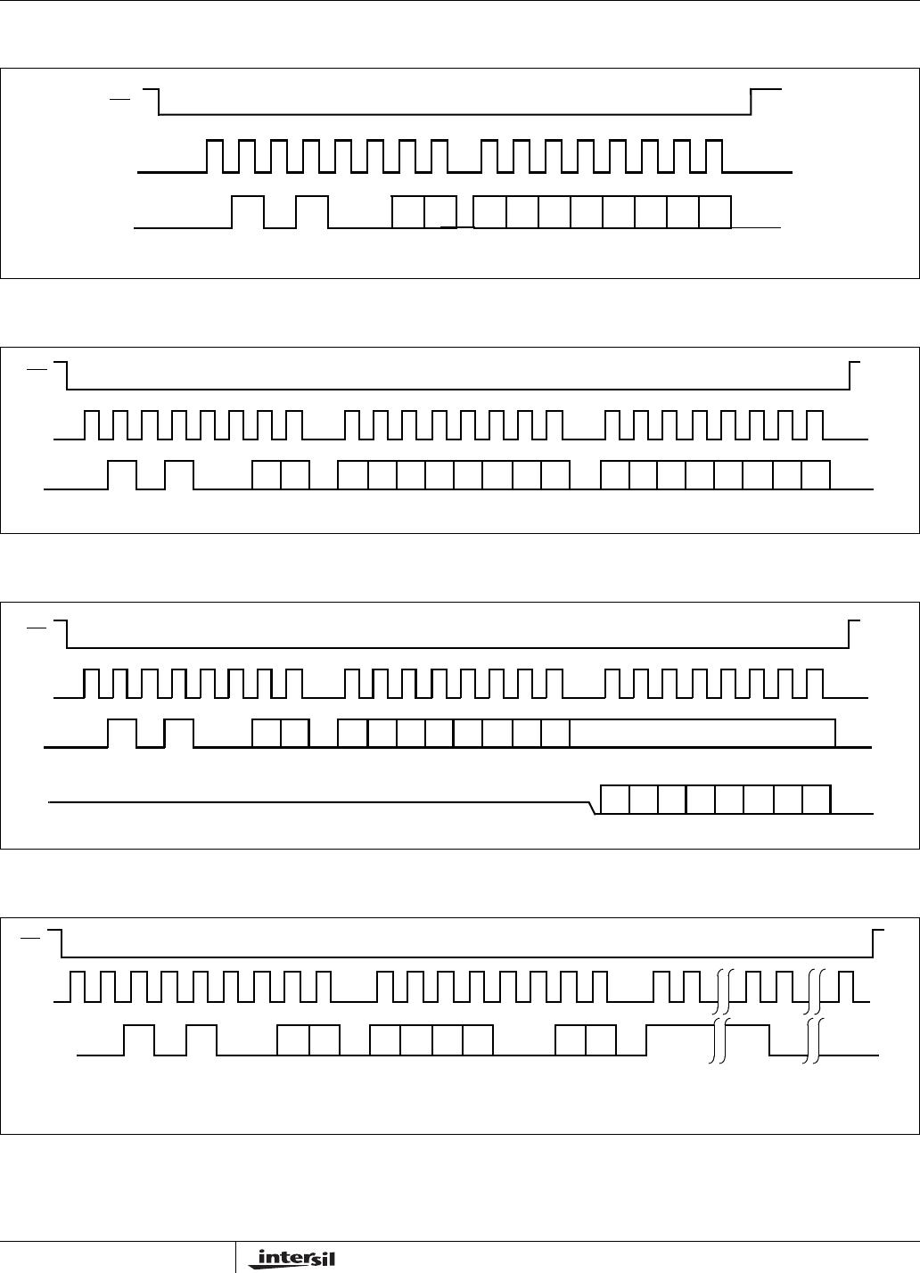
SCK
SI
V
W
/R
W
INC/DEC CMD Issued
t
WRID
Voltage Out
X9250
9
FN8165.3
August 29, 2006
Instruction Format
Notes: (1) “A1 ~ A0”: stands for the device addresses sent by the master.
(2) WPx refers to wiper position data in the Counter Register
(2) “I”: stands for the increment operation, SI held HIGH during active SCK phase (high).
(3) “D”: stands for the decrement operation, SI held LOW during active SCK phase (high).
Read Wiper Counter Register(WCR)
Write Wiper Counter Register (WCR)
Read Data Register (DR)
Write Data Register (DR)
Transfer Data Register (DR) to Wiper Counter Register (WCR)
CS
Falling
Edge
device type
identifier
device
addresses
instruction
opcode
WCR
addresses
wiper position
(sent by X9250 on SO)
CS
Rising
Edge
010100
A
1
A
0
100100
P
1
P
0
W
P
7
W
P
6
W
P
5
W
P
4
W
P
3
W
P
2
W
P
1
W
P
0
CS
Falling
Edge
device type
identifier
device
addresses
instruction
opcode
WCR
addresses
Data Byte
(sent by Host on SI)
CS
Rising
Edge
010100
A
1
A
0
101000
P
1
P
0
W
P
7
W
P
6
W
P
5
W
P
4
W
P
3
W
P
2
W
P
1
W
P
0
CS
Falling
Edge
device type
identifier
device
addresses
instruction
opcode
DR and WCR
addresses
Data Byte
(sent by X9250 on SO)
CS
Rising
Edge
010100
A
1
A
0
1011
R
1
R
0
P
1
P
0
W
P
7
W
P
6
W
P
5
W
P
4
W
P
3
W
P
2
W
P
1
W
P
0
CS
Falling
Edge
device type
identifier
device
addresses
instruction
opcode
DR and WCR
addresses
Data Byte
(sent by host on SI)
CS
Rising
Edge
HIGH-VOLTAGE
WRITE CYCLE
010100
A
1
A
0
1100
R
1
R
0
P
1
P
0
W
P
7
W
P
6
W
P
5
W
P
4
W
P
3
W
P
2
W
P
1
W
P
0
CS
Falling
Edge
device type
identifier
device
addresses
instruction
opcode
DR and WCR
addresses
CS
Rising
Edge
010100
A
1
A
0
1101R1R0P1P0
X9250

X9250US24Z-2.7

Mfr. #:
Manufacturer:
Renesas / Intersil
Description:
Digital Potentiometer ICs SPI XDCP 100K QD 256 TAPS
Lifecycle:
New from this manufacturer.
Delivery:
DHL FedEx Ups TNT EMS
Payment:
T/T Paypal Visa MoneyGram Western Union