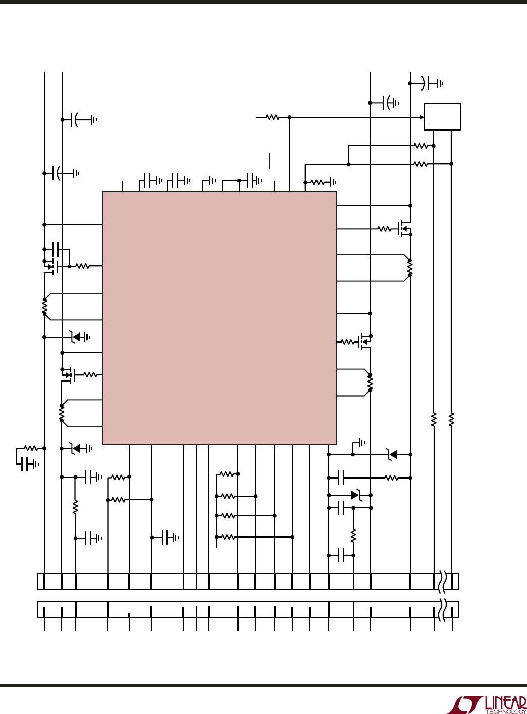
LTC4245
13
4245fa
OPERATIO
U
Start-Up
The LTC4245 is designed to turn a board’s supply voltages
on and off in a controlled manner, allowing the board to be
safely inserted or removed from a live backplane slot. When
a supply turn-on command is received, current sources
start pulling up the TIMER and SS pins. The 100μA I
TMR
current and the external TIMER capacitor determine the
time a supply can be in current limit during start-up. The
gate of a supply’s external N-channel MOSFET is servoed
by an amplifer (ACL
n
) so that the current, as indicated by
the sense resistor voltage drop, never exceeds an internal
current limit. This current limit rises at a rate determined
by I
SS
and the capacitor at the SS pin. A foldback circuit
determines the maximum value of the current limit and
reduces it to 30% of the maximum when a supply’s output
is shorted to ground. When the TIMER pin crosses 2.56V
it is reset to ground and the start-up timing cycle ends. If
a supply is still in current limit all gates are turned off, an
overcurrent fault is logged and the TIMER goes through
a cool-down timing cycle using 2μA for I
TMR
. Otherwise,
its circuit breaker (ECB
n
) is armed and the current limit
is raised to 3 times the circuit breaker threshold. The SS
pin is then reset by switch M2.
Any combination of the four supplies can be turned on
together or one after another. Whenever a supply is ramp-
ing up, its output voltage will affect, through the foldback
circuit, where the internal current limit ramp stops. The
default confi guration turns on all supplies together. If
sequence control bit C6 (Table 9) is set, the supplies turn
on in a 12V, 5V, 3.3V, –12V sequence. With this bit set,
the end of a supply ramp-up triggers the start of the next
one in the sequence. The I
2
C interface allows independent
on and off control for each supply through its On control
bit. Turn-off is simultaneous under fault conditions and
when using the ON or BD_SEL# pins.
At the end of the last start-up timing cycle, HEALTHY#
is pulled low by M3 if all supply outputs are above their
power bad thresholds. LOCAL_PCI_RST# which was held
low (M4), now follows PCI_RST#. The TIMER pin goes
through a PGI timeout cycle using 10μA for I
TMR
. The PGI
pin is sampled at the end of the cycle. If it is low, then
all external MOSFETs are shut-off, a PGI fault is logged
and TIMER goes through a cool-down cycle using 2μA
for I
TMR
. If PGI is high, the part enters the normal mode
of operation.
Normal Operation
During normal operation, the gates of the MOSFETs are
clamped about 6.2V above their sources. The 12V gate
driver uses a charge pump, the 5V and 3.3V gate drive is
derived from 12V
IN
and the –12V gate drive from INTV
CC
.
Each supply is continuously monitored for undervoltage,
overcurrent and power bad conditions. Overcurrent moni-
toring consists of an electronic circuit breaker comparator
(ECB
n
) and an active current limit circuit (ACL
n
) set at 3x the
ECB threshold. Undervoltage and overcurrent faults cause
all MOSFETs to be shut off. A power bad condition causes
HEALTHY# to go high impedance and LOCAL_PCI_RST#
to pull low, without shutting off the MOSFETs. If the PGI
pin is not disabled (register bit C3 not set), then PGI pin
going low will also shut off all MOSFETs.
ADC
Included in the LTC4245 is an 8-bit A/D converter. The
converter has a 13-input multiplexer to select between
input, output and current sense voltage of each supply,
and the GPIO channel. The ADC can either cycle through
all channels or measure a channel on-demand.
Serial Interface
An I
2
C interface is provided to read from or write to the
status, control and A/D registers. It allows the host to poll
the device and determine if faults have occurred. If the
ALERT# line is used as an interrupt, the host can respond
to a fault in real time. The LTC4245 I
2
C interface slave ad-
dress is decoded using the ADR0 to ADR3 pins.
Confi guration, GPIO and Precharge
The three-state CFG pin can be used to disable the V
EE
undervoltage lockout, power bad and foldback functions.
It can also convert the 5V undervoltage, power bad and
ADC levels to 3.3V levels. The GPIO1 to GPIO3 pins can
be used as general purpose inputs or outputs (M5 to
M7). One of the pins can also be multiplexed to the GPIO
channel of the ADC. A 1V reference voltage derived from
3V
IN
is provided at the PRECHARGE pin. This can be used
to pre-charge I/O lines on the board so as not to corrupt
the backplane bus.
LTC4245
14
4245fa
APPLICATIO S I FOR ATIO
WUU
U
ALERT#
SCL
SDA
HEALTHY#
12V
600mA
3.3V
7A
–12V
300mA
5V
5A
BOARD
CONNECTOR
(FEMALE)
BACKPLANE
CONNECTOR
(MALE)
BD_SEL#
PRECHARGE
LTC4245G
12V
MEDIUM 5V
BD_SEL#
HEALTHY#
SDA
SCL
ALERT#
MEDIUM 3.3V
–12V
I/O PIN 1
I/O PIN 128
I/O DATA LINE 128
I/O DATA LINE 1
R11
1
R19
1.74
Q4, Si4872
R4
100m
R1
50m
R2, 3.5m
R18, 2.74
R10
1
R3
2.5m
Q3, Si7880DP
R24
10k
R21
10
R20
10
GPIO1
5V
IN
5V
SENSE
5V
OUT
12V
OUT
12V
IN
12V
SENSE
12V
GATE
5V
GATE
3V
SENSE
3V
IN
3V
GATE
3V
OUT
V
EEIN
V
EESENSE
V
EEGATE
V
EEOUT
LONG 5V
LONG V(I/0)
+
+
+
TIMER
CFG
SS
+
R12
10k
R7
10
R8
10
R9
18
R22
10k
R23
10k
Z3
Z4
Z2 Z1
22
36 35 34 33 5 6 7 8
21 20 19 16 15
23
14
13
12
1
10
26
28
3
11
4
2
27
24
17 18
3V
IN
ADR3
GA[3]
32
GND
9
GROUND
LONG 3.3V
PCI_RST#
25
PCI_RST#
R13
10k
ADR2
GA[2]
31
R14
10k
ADR1
GA[1]
30
R15
10k
R6
10
R5
10
R16
10k
ADR0
GA[0]
29
R17
1.2k
ON
PGI
INTV
CC
LOCAL_PCI_RST#
RESET
PCI
BRIDGE
CHIP
C1
0.1 µF
C2
10nF
C
L
(3V
OUT
)
2200 µF
C
L(VEEOUT)
100 µF
C
T
2.2 µF
C
SS
220nF
ADC INPUT
TO RESET OF
SUPPLY MONITOR
C
L(12V
OUT
)
100 µF
C
L(5V
OUT
)
2200 µF
Q1, IRF7413
Q2, Si788ODP
C4
Z1
, Z4: DIODES INC. SMAJ12A
Z2
, Z3: DIODES INC. SMAJ5.0A
4245 FO1
3V
OUT
C8
2.2nF
C9
10nF
C3
10nF
C7C6
C5
10nF
PER PIN
10nF
PER PIN
Figure 1. CompactPCI Application
LTC4245
15
4245fa
The typical LTC4245 application is in a high availability sys-
tem where boards using multiple supplies are hot plugged.
The device enables the system to periodically monitor board
power consumption and fault status over the I
2
C interface.
Boards in CompactPCI and PCI Express systems typically
utilize three to four supplies. Figure 1 shows the LTC4245
being used in a CompactPCI application.
The following sections describe the turn on, turn off and
fault response behavior of the LTC4245. The ADC and I
2
C
interface are discussed next. External component selection
is discussed in detail in the Design Example section.
CPCI Connection Pin Sequence
The staggered lengths of the CPCI male connector pins on
the backplane ensures that all power supplies are physi-
cally connected to the LTC4245 before back-end power
is allowed to ramp up (BD_SEL# asserted low). The long
pins, which include 5V, 3.3V, V(I/O) and GND, mate fi rst.
The short BD_SEL# pin mates last. At least one long 3.3V
power pin must be connected to the LTC4245 in order for
the PRECHARGE pin voltage to be available before the
CPCI bus pins mate.
The following is a typical hot plug sequence.
1. ESD clips make contact.
2. Long power and ground pins make contact and Early
Power is established. The 1V precharge voltage
becomes valid at this stage. Power is also applied
to the pull-up resistors connected to the HEALTHY#
and BD_SEL# signals. LOCAL_PCI_RST# is held
in reset. All power switches are held off at this stage
of insertion.
3. Medium length pins make contact. The 12V and –12V
connector pins make contact at this stage. The
internal low voltage supply of the LTC4245 (INTV
CC
)
powers up from the 12V supply. An internal 10μA
pull-up from INTV
CC
to BD_SEL# turns on. Other
connector pins that mate are HEALTHY#, PCI_RST#
and the bus I/O pins (which are precharged to 1V).
4. Short pins make contact. If the BD_SEL# signal is
grounded on the backplane, the plug-in board
power-up cycle may begin immediately. If the ON pin
is tied high then turn-on is automatic, else the LTC4245
waits for a serial bus turn-on command. System
backplanes that do not ground the BD_SEL# signal
will instead have circuitry that detects when
BD_SEL# makes contact with the plug-in board. The
system logic can then control the power up process
by pulling BD_SEL# low. The precharge potential may
be optionally disconnected from the CPCI bus signals
at this stage.
Turn-On
The back-end power planes are isolated from the input
power planes by external N-channel pass transistors Q1
through Q4. Sense resistors R1 to R4 provide current
fault detection. Resistors R5 to R8 prevent high frequency
oscillations in MOSFETs Q1 to Q4 respectively.
The following conditions must be satisfi ed for a duration of
100ms before the external switches can be turned on.
1. All input supplies and the internally generated supply,
INTV
CC
, must exceed their undervoltage lockout
thresholds. The V
EE
undervoltage lockout can be
disabled by not tying the CFG pin low.
2. No undervoltage, overcurrent or PGI fault bits must
be set unless the corresponding auto-retry is enabled.
When 12V
IN
powers up for the fi rst time, INTV
CC
rises above its undervoltage threshold which
generates a 60μs to 120μs internal power-on-reset
pulse. During reset, the fault registers are cleared
and the control bits are initialized. If INTV
CC
is already
up, then the I
2
C interface can be used to clear the
fault bits or set the auto-retry bits.
3. The BD_SEL# pin must be pulled low.
When these initial conditions are satisfi ed, the ON pin is
checked. If it is high, the four FET On control bits (D0 to
D3) are set either simultaneously (the default state) or
in a 12V, 5V, 3.3V, –12V sequence (register bit C6 set).
If ON is low, the external switches turn on when the ON
pin is brought high or if a serial bus turn-on command
is received. Figure 2 shows all supplies turning on after
BD_SEL# goes low.
APPLICATIO S I FOR ATIO
WUU
U

LTC4245IG#PBF

Mfr. #:
Manufacturer:
Analog Devices Inc.
Description:
Hot Swap Voltage Controllers Quad Hot Swap Contr. w/ADC and I2C
Lifecycle:
New from this manufacturer.
Delivery:
DHL FedEx Ups TNT EMS
Payment:
T/T Paypal Visa MoneyGram Western Union