REV. 0
Information furnished by Analog Devices is believed to be accurate and
reliable. However, no responsibility is assumed by Analog Devices for its
use, nor for any infringements of patents or other rights of third parties
which may result from its use. No license is granted by implication or
otherwise under any patent or patent rights of Analog Devices.
a
AD5334/AD5335/AD5336/AD5344*
One Technology Way, P.O. Box 9106, Norwood, MA 02062-9106, U.S.A.
Tel: 781/329-4700 World Wide Web Site: http://www.analog.com
Fax: 781/326-8703 © Analog Devices, Inc., 2000
2.5 V to 5.5 V, 500 A, Parallel Interface
Quad Voltage-Output 8-/10-/12-Bit DACs
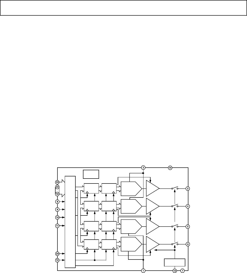
AD5334 FUNCTIONAL BLOCK DIAGRAM
(Other Diagrams Inside)
V
OUT
A
BUFFER
GND
AD5334
V
OUT
B
BUFFER
V
OUT
C
BUFFER
V
OUT
D
BUFFER
POWER-ON
RESET
TO ALL DACS
AND BUFFERS
POWER-DOWN
LOGIC
PD
DAC
REGISTER
8-BIT
DAC
8-BIT
DAC
INPUT
REGISTER
V
REF
C/D
INTER-
FACE
LOGIC
V
DD
V
REF
A/B
GAIN
DB
7
DB
0
CS
WR
A0
A1
CLR
LDAC
.
.
.
DAC
REGISTER
INPUT
REGISTER
DAC
REGISTER
INPUT
REGISTER
DAC
REGISTER
INPUT
REGISTER
8-BIT
DAC
8-BIT
DAC
8-BIT
DAC
FEATURES
AD5334: Quad 8-Bit DAC in 24-Lead TSSOP
AD5335: Quad 10-Bit DAC in 24-Lead TSSOP
AD5336: Quad 10-Bit DAC in 28-Lead TSSOP
AD5344: Quad 12-Bit DAC in 28-Lead TSSOP
Low Power Operation: 500 A @ 3 V, 600 A @ 5 V
Power-Down to 80 nA @ 3 V, 200 nA @ 5 V via PD Pin
2.5 V to 5.5 V Power Supply
Double-Buffered Input Logic
Guaranteed Monotonic by Design Over All Codes
Output Range: 0–V
REF
or 0–2 V
REF
Power-On Reset to Zero Volts
Simultaneous Update of DAC Outputs via LDAC Pin
Asynchronous CLR Facility
Low Power Parallel Data Interface
On-Chip Rail-to-Rail Output Buffer Amplifiers
Temperature Range: –40C to +105C
APPLICATIONS
Portable Battery-Powered Instruments
Digital Gain and Offset Adjustment
Programmable Voltage and Current Sources
Programmable Attenuators
Industrial Process Control
GENERAL DESCRIPTION
The AD5334/AD5335/AD5336/AD5344 are quad 8-, 10-, and
12-bit DACs. They operate from a 2.5 V to 5.5 V supply con-
suming just 500 µA at 3 V, and feature a power-down mode that
further reduces the current to 80 nA. These devices incorporate
an on-chip output buffer that can drive the output to both sup-
ply rails.
The AD5334/AD5335/AD5336/AD5344 have a parallel interface.
CS selects the device and data is loaded into the input registers
on the rising edge of WR.
The GAIN pin on the AD5334 and AD5336 allows the output
range to be set at 0 V to V
REF
or 0 V to 2 × V
REF
.
Input data to the DACs is double-buffered, allowing simultaneous
update of multiple DACs in a system using the LDAC pin.
On the AD5334, AD5335 and AD5336 an asynchronous CLR
input is also provided. This resets the contents of the Input
Register and the DAC Register to all zeros. These devices also
incorporate a power-on-reset circuit that ensures that the DAC
output powers on to 0 V and remains there until valid data is
written to the device.
The AD5334/AD5335/AD5336/AD5344 are available in Thin
Shrink Small Outline Packages (TSSOP).
*Protected by U.S. Patent Number 5,969,657
.
REV. 0
–2–
AD5334/AD5335/AD5336/AD5344–SPECIFICATIONS
(V
DD
= 2.5 V to 5.5 V, V
REF
= 2 V. R
L
= 2 k to GND; C
L
=200 pF to GND; all specifications T
MIN
to T
MAX
unless otherwise noted.)
B Version
2
Parameter
1
Min Typ Max Unit Conditions/Comments
DC PERFORMANCE
3, 4
AD5334
Resolution 8 Bits
Relative Accuracy ± 0.15 ± 1 LSB
Differential Nonlinearity ± 0.02 ± 0.25 LSB Guaranteed Monotonic By Design Over All Codes
AD5335/AD5336
Resolution 10 Bits
Relative Accuracy ± 0.5 ± 4 LSB
Differential Nonlinearity ± 0.05 ± 0.5 LSB Guaranteed Monotonic By Design Over All Codes
AD5344
Resolution 12 Bits
Relative Accuracy ± 2 ± 16 LSB
Differential Nonlinearity ± 0.2 ± 1 LSB Guaranteed Monotonic By Design Over All Codes
Offset Error ± 0.4 ± 3 % of FSR
Gain Error ± 0.1 ± 1 % of FSR
Lower Deadband
5
10 60 mV Lower Deadband Exists Only if Offset Error Is Negative
Upper Deadband 10 60 mV V
DD
= 5 V. Upper Deadband Exists Only if V
REF =
V
DD
Offset Error Drift
6
–12 ppm of FSR/°C
Gain Error Drift
6
–5 ppm of FSR/°C
DC Power Supply Rejection Ratio
6
–60 dB V
DD
= ±10%
DC Crosstalk
6
200 µVR
L
= 2 k to GND, 2 k to V
DD
; C
L
= 200 pF to GND;
Gain = 0
DAC REFERENCE INPUT
6
V
REF
Input Range 0.25 V
DD
V
V
REF
Input Impedance 180 k Gain = 1. Input Impedance = R
DAC
(AD5336/AD5344)
90 k Gain = 2. Input Impedance = R
DAC
(AD5336)
90 k Gain = 1. Input Impedance = R
DAC
(AD5334/AD5335)
45 k Gain = 2. Input Impedance = R
DAC
(AD5334)
Reference Feedthrough –90 dB Frequency = 10 kHz
Channel-to-Channel Isolation –90 dB Frequency = 10 kHz
OUTPUT CHARACTERISTICS
6
Minimum Output Voltage
4, 7
0.001 V min Rail-to-Rail Operation
Maximum Output Voltage
4, 7
V
DD
– 0.001 V max
DC Output Impedance 0.5
Short Circuit Current 50 mA V
DD
= 5 V
20 mA V
DD
= 3 V
Power-Up Time 2.5 µs Coming Out of Power-Down Mode. V
DD
= 5 V
5 µs Coming Out of Power-Down Mode. V
DD
= 3 V
LOGIC INPUTS
6
Input Current ± 1 µA
V
IL
, Input Low Voltage 0.8 V V
DD
= 5 V ± 10%
0.6 V V
DD
= 3 V ± 10%
0.5 V V
DD
= 2.5 V
V
IH
, Input High Voltage 2.4 V V
DD
= 5 V ± 10%
2.1 V V
DD
= 3 V ± 10%
2.0 V V
DD
= 2.5 V
Pin Capacitance 3.5 pF
POWER REQUIREMENTS
V
DD
2.5 5.5 V
I
DD
(Normal Mode) All DACs active and excluding load currents.
V
DD
= 4.5 V to 5.5 V 600 900 µAV
IH
= V
DD
, V
IL
= GND.
V
DD
= 2.5 V to 3.6 V 500 700 µAI
DD
increases by 50 µA at V
REF
> V
DD
– 100 mV.
I
DD
(Power-Down Mode)
V
DD
= 4.5 V to 5.5 V 0.2 1 µA
V
DD
= 2.5 V to 3.6 V 0.08 1 µA
NOTES
1
See Terminology section.
2
Temperature range: B Version: –40°C to +105°C; typical specifications are at 25°C.
3
Linearity is tested using a reduced code range: AD5334 (Code 8 to 255); AD5335/AD5336 (Code 28 to 1023); AD5344 (Code 115 to 4095).
4
DC specifications tested with outputs unloaded.
5
This corresponds to x codes. x = Deadband voltage/LSB size.
6
Guaranteed by design and characterization, not production tested.
7
In order for the amplifier output to reach its minimum voltage, Offset Error must be negative. In order for the amplifier output to reach its maximum voltage, V
REF
= V
DD
and
“Offset plus Gain” Error must be positive.
Specifications subject to change without notice.
REV. 0
–3–
AD5334/AD5335/AD5336/AD5344
AC CHARACTERISTICS
1
B Version
3
Parameter
2
Min Typ Max Unit Conditions/Comments
Output Voltage Settling Time V
REF
= 2 V. See Figure 20
AD5334 6 8 µs 1/4 Scale to 3/4 Scale Change (40 H to C0 H)
AD5335 7 9 µs 1/4 Scale to 3/4 Scale Change (100 H to 300 H)
AD5336 7 9 µs 1/4 Scale to 3/4 Scale Change (100 H to 300 H)
AD5344 8 10 µs 1/4 Scale to 3/4 Scale Change (400 H to C00 H)
Slew Rate 0.7 V/µs
Major Code Transition Glitch Energy 8 nV-s 1 LSB Change Around Major Carry
Digital Feedthrough 0.5 nV-s
Digital Crosstalk 3 nV-s
Analog Crosstalk 0.5 nV-s
DAC-to-DAC Crosstalk 3.5 nV-s
Multiplying Bandwidth 200 kHz V
REF
= 2 V ± 0.1 V p-p. Unbuffered Mode
Total Harmonic Distortion –70 dB V
REF
= 2.5 V ± 0.1 V p-p. Frequency = 10 kHz
NOTES
1
Guaranteed by design and characterization, not production tested.
2
See Terminology section.
3
Temperature range: B Version: –40°C to +105°C; typical specifications are at 25°C.
Specifications subject to change without notice.
TIMING CHARACTERISTICS
1, 2, 3
Parameter Limit at T
MIN
, T
MAX
Unit Condition/Comments
t
1
0 ns min CS to WR Setup Time
t
2
0 ns min CS to WR Hold Time
t
3
20 ns min WR Pulsewidth
t
4
5 ns min Data, GAIN, HBEN Setup Time
t
5
4.5 ns min Data, GAIN, HBEN Hold Time
t
6
5 ns min Synchronous Mode. WR Falling to LDAC Falling.
t
7
5 ns min Synchronous Mode. LDAC Falling to WR Rising.
t
8
4.5 ns min Synchronous Mode. WR Rising to LDAC Rising.
t
9
5 ns min Asynchronous Mode. LDAC Rising to WR Rising.
t
10
4.5 ns min Asynchronous Mode. WR Rising to LDAC Falling.
t
11
20 ns min LDAC Pulsewidth
t
12
20 ns min CLR Pulsewidth
t
13
50 ns min Time Between WR Cycles
t
14
20 ns min A0, A1 Setup Time
t
15
0 ns min A0, A1 Hold Time
NOTES
1
Guaranteed by design and characterization, not production tested.
2
All input signals are specified with tr = tf = 5 ns (10% to 90% of V
DD
)
and timed from a voltage level of (V
IL
+ V
IH
)/2.
3
See Figure 1.
Specifications subject to change without notice.
(V
DD
= 2.5 V to 5.5 V. R
L
= 2 k to GND; C
L
= 200 pF to GND. All specifications T
MIN
to T
MAX
unless other-
wise noted.)
t
15
t
14
t
8
CS
WR
DATA,
GAIN,
HBEN
LDAC
1
LDAC
2
CLR
NOTES:
1
SYNCHRONOUS LDAC UPDATE MODE
2
ASYNCHRONOUS LDAC UPDATE MODE
A0,
A1
t
1
t
2
t
5
t
3
t
13
t
4
t
7
t
6
t
9
t
10
t
11
t
12
Figure 1. Parallel Interface Timing Diagram
(V
DD
= 2.5 V to 5.5 V, All specifications T
MIN
to T
MAX
unless otherwise noted.)

AD5336BRU

Mfr. #:
Manufacturer:
Analog Devices Inc.
Description:
Digital to Analog Converters - DAC Quad 10-Bit
Lifecycle:
New from this manufacturer.
Delivery:
DHL FedEx Ups TNT EMS
Payment:
T/T Paypal Visa MoneyGram Western Union