REV. 0
AD5334/AD5335/AD5336/AD5344
–10–
OFFSET ERROR DRIFT
This is a measure of the change in Offset Error with changes in
temperature. It is expressed in (ppm of full-scale range)/°C.
GAIN ERROR DRIFT
This is a measure of the change in Gain Error with changes in
temperature. It is expressed in (ppm of full-scale range)/°C.
DC POWER-SUPPLY REJECTION RATIO (PSRR)
This indicates how the output of the DAC is affected by changes in
the supply voltage. PSRR is the ratio of the change in V
OUT
to a
change in V
DD
for full-scale output of the DAC. It is measured
in dBs. V
REF
is held at 2 V and V
DD
is varied ±10%.
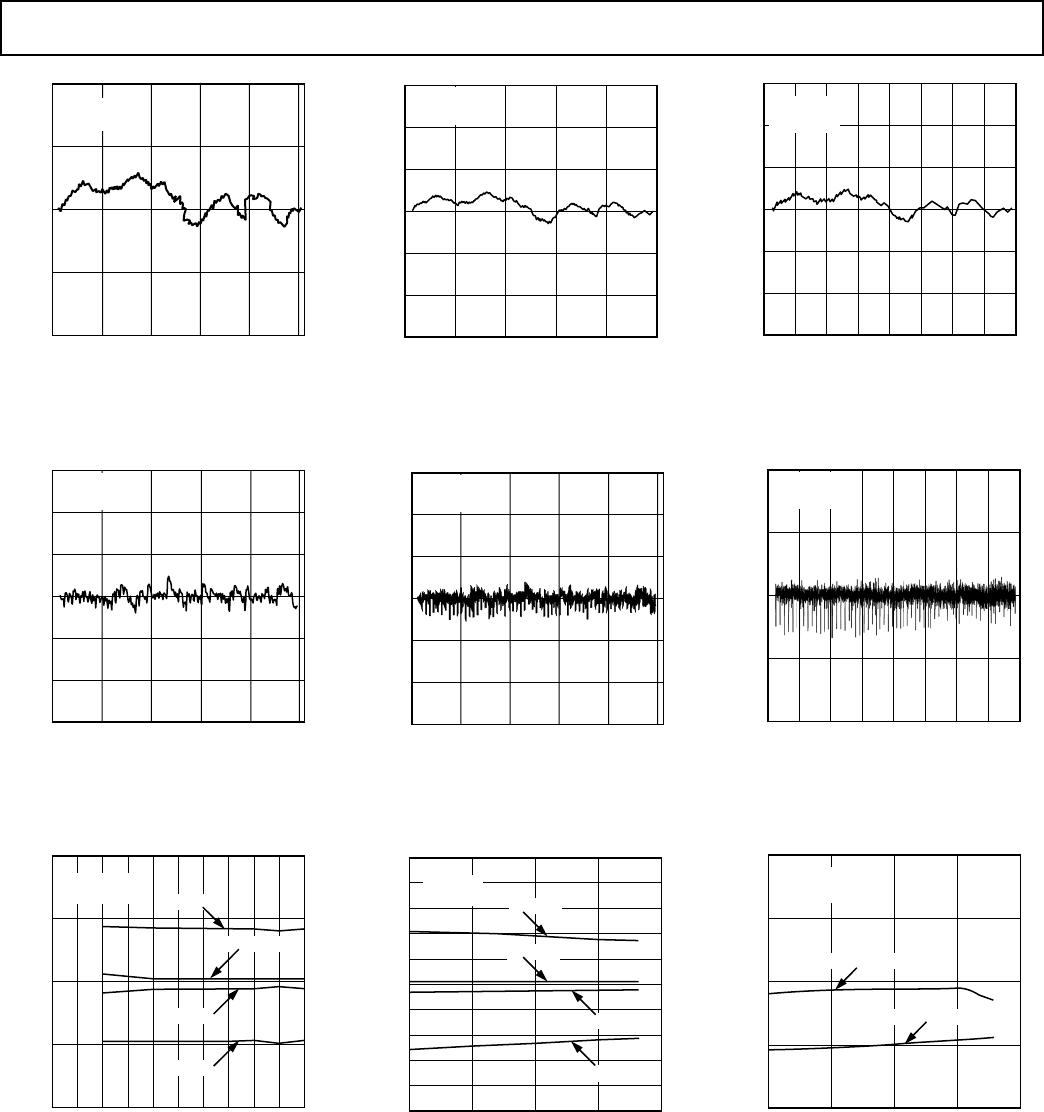
DC CROSSTALK
This is the dc change in the output level of one DAC at mid-
scale in response to a full-scale code change (all 0s to all 1s and
vice versa) and output change of another DAC. It is expressed
in µV.
REFERENCE FEEDTHROUGH
This is the ratio of the amplitude of the signal at the DAC output
to the reference input when the DAC output is not being updated
(i.e., LDAC is high). It is expressed in dBs.
CHANNEL-TO-CHANNEL ISOLATION
This is a ratio of the amplitude of the signal at the output of one
DAC to a sine wave on the reference inputs of the other DACs.
It is measured by grounding one V
REF
pin and applying a 10 kHz,
4 V peak-to-peak sine wave to the other V
REF
pins. It is expressed
in dBs.
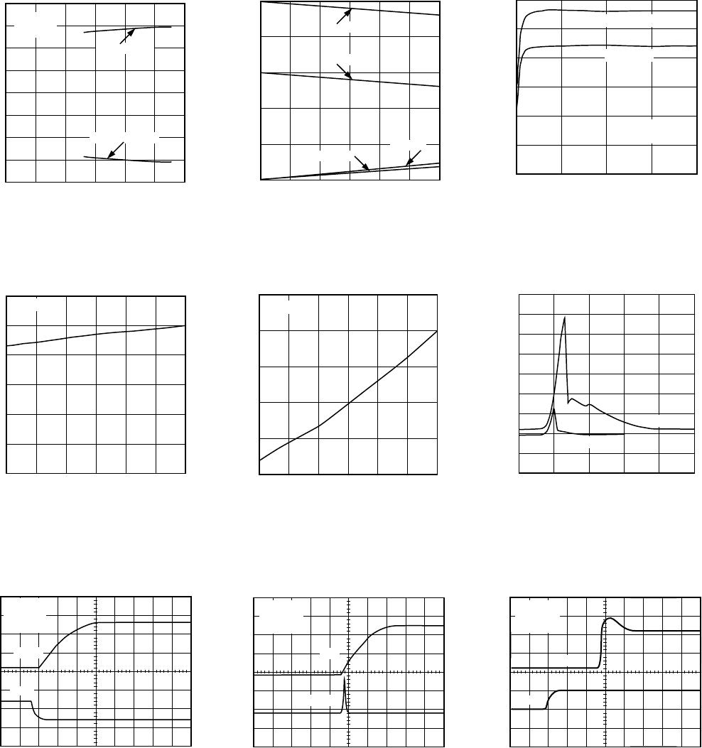
MAJOR-CODE TRANSITION GLITCH ENERGY
Major-Code Transition Glitch Energy is the energy of the
impulse injected into the analog output when the DAC changes
state. It is normally specified as the area of the glitch in nV secs
and is measured when the digital code is changed by 1 LSB at
the major carry transition (011 . . . 11 to 100 . . . 00 or 100 . . . 00
to 011 . . . 11).
DIGITAL FEEDTHROUGH
Digital Feedthrough is a measure of the impulse injected into
the analog output of the DAC from the digital input pins of the
device but is measured when the DAC is not being written to
(CS held high). It is specified in nV-secs and is measured with a
full-scale change on the digital input pins, i.e. from all 0s to all
1s and vice versa.
DIGITAL CROSSTALK
This is the glitch impulse transferred to the output of one DAC
at midscale in response to a full-scale code change (all 0s to all
1s and vice versa) in the input register of another DAC. It is
expressed in nV secs.
ANALOG CROSSTALK
This is the glitch impulse transferred to the output of one DAC
due to a change in the output of another DAC. It is measured
by loading one of the input registers with a full-scale code change
(all 0s to all 1s and vice versa) while keeping LDAC high. Then
pulse LDAC low and monitor the output of the DAC whose
digital code was not changed. The area of the glitch is expressed
in nV secs.
DAC-TO-DAC CROSSTALK
This is the glitch impulse transferred to the output of one DAC
due to a digital code change and subsequent output change of
another DAC. This includes both digital and analog crosstalk. It
is measured by loading one of the DACs with a full-scale code
change (all 0s to all 1s and vice versa) with the LDAC pin set
low and monitoring the output of another DAC. The energy of
the glitch is expressed in nV secs.
MULTIPLYING BANDWIDTH
The amplifiers within the DAC have a finite bandwidth. The
Multiplying Bandwidth is a measure of this. A sine wave on the
reference (with full-scale code loaded to the DAC) appears on
the output. The Multiplying Bandwidth is the frequency at which
the output amplitude falls to 3 dB below the input.
TOTAL HARMONIC DISTORTION
This is the difference between an ideal sine wave and its attenuated
version using the DAC. The sine wave is used as the reference
for the DAC and the THD is a measure of the harmonics present
on the DAC output. It is measured in dBs.