REV. 0
AD5334/AD5335/AD5336/AD5344
–17–
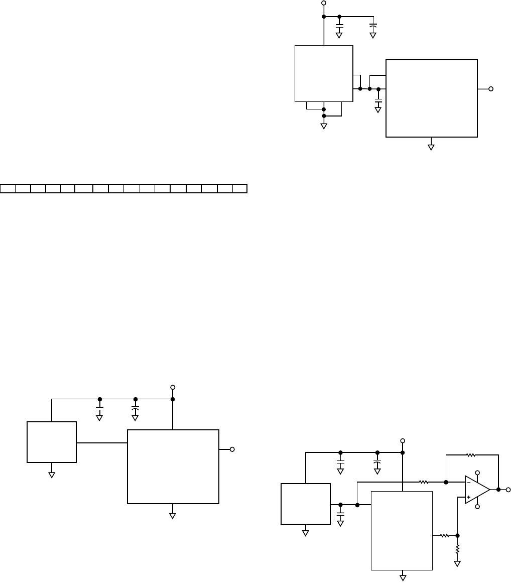
Decoding Multiple AD5334/AD5335/AD5336/AD5344
The CS pin on these devices can be used in applications to decode
a number of DACs. In this application, all DACs in the system
receive the same data and WR pulses, but only the CS to one of
the DACs will be active at any one time, so data will only be
written to the DAC whose CS is low. If multiple AD5343s are
being used, a common HBEN line will also be required to
determine if the data is written to the high-byte or low-byte
register of the selected DAC.
The 74HC139 is used as a 2- to 4-line decoder to address any
of the DACs in the system. To prevent timing errors from oc-
curring, the enable input should be brought to its inactive state
while the coded address inputs are changing state. Figure 36 shows
a diagram of a typical setup for decoding multiple devices in a
system. Once data has been written sequentially to all DACs in
a system, all the DACs can be updated simultaneously using a
common LDAC line. A common CLR line can also be used to
reset all DAC outputs to zero (except on the AD5344).
ENABLE
CODED
ADDRESS
1G
1A
1B
V
DD
V
CC
74HC139
DGND
1Y0
1Y1
1Y2
1Y3
A0
A1
HBEN
WR
LDAC
CLR
DATA
INPUTS
DATA
INPUTS
DATA
INPUTS
A1
A0
HBEN*
WR
LDAC
CLR
CS
DATA
INPUTS
DATA BUS
*AD5335 ONLY
A1
A0
HBEN*
WR
LDAC
CLR
CS
A1
A0
HBEN*
WR
LDAC
CLR
CS
A1
A0
HBEN*
WR
LDAC
CLR
CS
AD5334/AD5335/
AD5336/AD5344
AD5334/AD5335/
AD5336/AD5344
AD5334/AD5335/
AD5336/AD5344
AD5334/AD5335/
AD5336/AD5344
Figure 36. Decoding Multiple DAC Devices
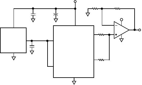
AD5334/AD5335/AD5336/AD5344 as a Digitally Programmable
Window Detector
A digitally programmable upper/lower limit detector using two
of the DACs in the AD5334/AD5335/AD5336/AD5344 is
shown in Figure 37.
Any pair of DACs in the device may be used, but for simplicity
the description will refer to DACs A and B.
Care must be taken to connect the correct reference inputs to
the reference source. The AD5334 and AD5335 have only two
reference inputs, V
REF
A/B for DACs A and B and V
REF
C/D for
DACs C and D. If DACs A and B are used (for example) then
only V
REF
A/B is needed. DACs C and D and V
REF
C/D may be
used for some other purpose. The AD5336 and AD5344 have
separate reference inputs for each DAC.
The upper and lower limits for the test are loaded to DACs A
and B which, in turn, set the limits on the CMP04. If a signal at
the V
IN
input is not within the programmed window, an LED
will indicate the fail condition.
5V
0.1F
10F
AD5336/AD5344
GND
V
REF
A
V
DD
V
OUT
A
V
REF
B
V
OUT
B
V
IN
FAIL PASS
1k⍀ 1k⍀
PASS/
FAIL
1/6 74HC05
1/2
CMP04
V
REF
Figure 37. Programmable Window Detector
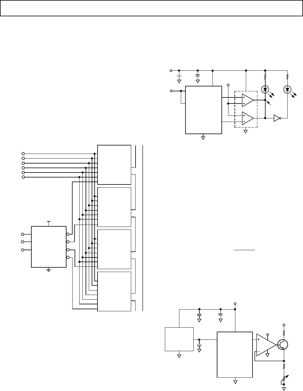
Programmable Current Source
Figure 38 shows the AD5334/AD5335/AD5336/AD5344 used
as the control element of a programmable current source. In this
example, the full-scale current is set to 1 mA. The output volt-
age from the DAC is applied across the current setting resistor
of 4.7 kΩ in series with the 470 Ω adjustment potentiometer,
which gives an adjustment of about ± 5%. Suitable transistors to
place in the feedback loop of the amplifier include the BC107
and the 2N3904, which enable the current source to operate
from a minimum V
SOURCE
of 6 V. The operating range is deter-
mined by the operating characteristics of the transistor. Suitable
amplifiers include the AD820 and the OP295, both having rail-
to-rail operation on their outputs. The current for any digital
input code and resistor value can be calculated as follows:
IGV
D
R
mA
REF
N
=× ×
×()2
Where:
G is the gain of the buffer amplifier (1 or 2)
D is the digital input code
N is the DAC resolution (8, 10, or 12 bits)
R is the sum of the resistor plus adjustment potentiometer in kΩ
AD5334/AD5335/
AD5336/AD5344
GND
V
DD
= 5V
EXT
REF
V
OUT
*
AD780/REF192
WITH V
DD
= 5V
GND
V
IN
V
OUT
V
REF
*
V
DD
4.7k⍀
5V
*ONLY ONE CHANNEL OF V
REF
AND V
OUT
SHOWN
0.1F
0.1F
10F
470⍀
LOAD
V
SOURCE
AD820/
OP295
Figure 38. Programmable Current Source