REV. 0
AD5334/AD5335/AD5336/AD5344
–14–
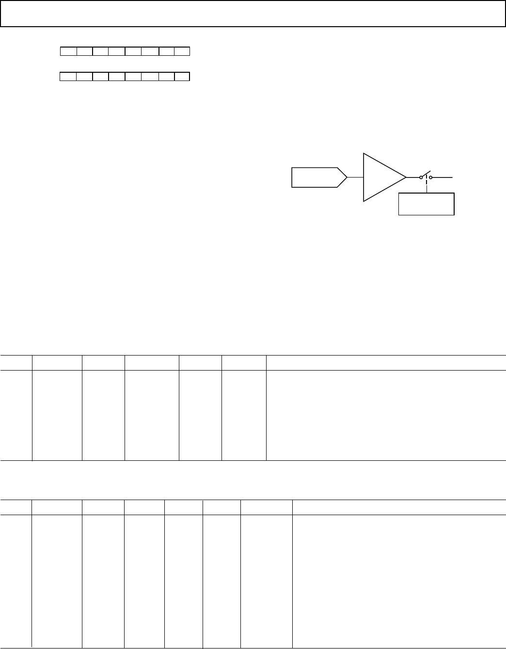
Resistor String
The resistor string section is shown in Figure 29. It is simply a
string of resistors, each of value R. The digital code loaded
to
the DAC register determines at what node on the string the
voltage is tapped off to be fed into the output amplifier. The
voltage is tapped off by closing one of the switches connecting
the string to the amplifier. Because it is a string of resistors, it is
guaranteed monotonic.
TO OUTPUT
AMPLIFIER
R
R
R
R
R
V
REF
Figure 29. Resistor String
DAC Reference Input
The DACs operate with an external reference. The reference
inputs are unbuffered and have an input range of 0.25 V to V
DD
.
The impedance per DAC is typically 180 kΩ for 0–V
REF
mode
and 90 kΩ for 0–2 V
REF
mode. The AD5336 and AD5344 have
separate reference inputs for each DAC, while the AD5334 and
AD5335 have a reference inputs for each pair of DACS (A/B
and C/D).
Output Amplifier
The output buffer amplifier is capable of generating output
voltages to within 1 mV of either rail. Its actual range depends
on V
REF
, GAIN, the load on V
OUT
, and offset error.
If a gain of 1 is selected (GAIN = 0), the output range is 0.001 V
to V
REF
.
If a gain of 2 is selected (GAIN = 1), the output range is 0.001 V
to 2 V
REF
. However because of clamping the maximum output
is limited to V
DD
– 0.001 V.
The output amplifier is capable of driving a load of 2 kΩ to
GND or V
DD
, in parallel with 500 pF to GND or V
DD
. The
source and sink capabilities of the output amplifier can be seen
in Figure 15.
The slew rate is 0.7 V/µs with a half-scale settling time to ± 0.5 LSB
(at 8 bits) of 6 µs with the output unloaded. See Figure 20.
PARALLEL INTERFACE
The AD5334, AD5336, and AD5344 load their data as a single
8-, 10-, or 12-bit word, while the AD5335 loads data as a low
byte of 8 bits and a high byte containing 2 bits.
Double-Buffered Interface
The AD5334/AD5335/AD5336/AD5344 DACs all have double-
buffered interfaces consisting of an input register and a DAC
register. DAC data and GAIN inputs (when available) are written
to the input register under control of the Chip Select (CS) and
Write (WR).
Access to the DAC register is controlled by the LDAC function.
When LDAC is high, the DAC register is latched and the input
register may change state without affecting the contents of the
DAC register. However, when LDAC is brought low, the DAC
register becomes transparent and the contents of the input
register are transferred to it. The gain control signal is also
double-buffered and is only updated when LDAC is taken low.
This is useful if the user requires simultaneous updating of all
DACs and peripherals. The user may write to all input registers
individually and then, by pulsing the LDAC input low, all out-
puts will update simultaneously.
Double-buffering is also useful where the DAC data is loaded in
two bytes, as in the AD5335, because it allows the whole data
word to be assembled in parallel before updating the DAC register.
This prevents spurious outputs that could occur if the DAC
register were updated with only the high byte or the low byte.
These parts contain an extra feature whereby the DAC register
is not updated unless its input register has been updated since
the last time that LDAC was brought low. Normally, when
LDAC is brought low, the DAC registers are filled with the
contents of the input registers. In the case of the AD5334/
AD5335/AD5336/AD5344, the part will only update the DAC
register if the input register has been changed since the last
time the DAC register was updated. This removes unnecessary
crosstalk.
Clear Input (CLR)
CLR is an active low, asynchronous clear that resets the input and
DAC registers. Note that the AD5344 has no CLR function.
Chip Select Input (CS)
CS is an active low input that selects the device.
Write Input (WR)
WR is an active low input that controls writing of data to the
device. Data is latched into the input register on the rising edge
of WR.
Load DAC Input (LDAC)
LDAC transfers data from the input register to the DAC register
(and hence updates the outputs). Use of the LDAC function
enables double buffering of the DAC and GAIN data. There
are two LDAC modes:
Synchronous Mode: In this mode the DAC register is updated
after new data is read in on the rising edge of the WR input.
LDAC can be tied permanently low or pulsed as in Figure 1.
Asynchronous Mode: In this mode the outputs are not updated
at the same time that the input register is written to. When LDAC
goes low the DAC register is updated with the contents of the
input register.
High-Byte Enable Input (HBEN)
High-Byte Enable is a control input on the AD5335 only that
determines if data is written to the high-byte input register or
the low-byte input register.
The low data byte of the AD5335 consists of data bits 0 to 7 at
data inputs DB
0
to DB
7
, while the high byte consists of Data
Bits 8 and 9 at data inputs DB
0
and DB
1
. DB
2
to DB
7
are
ignored during a high byte write. See Figure 30.