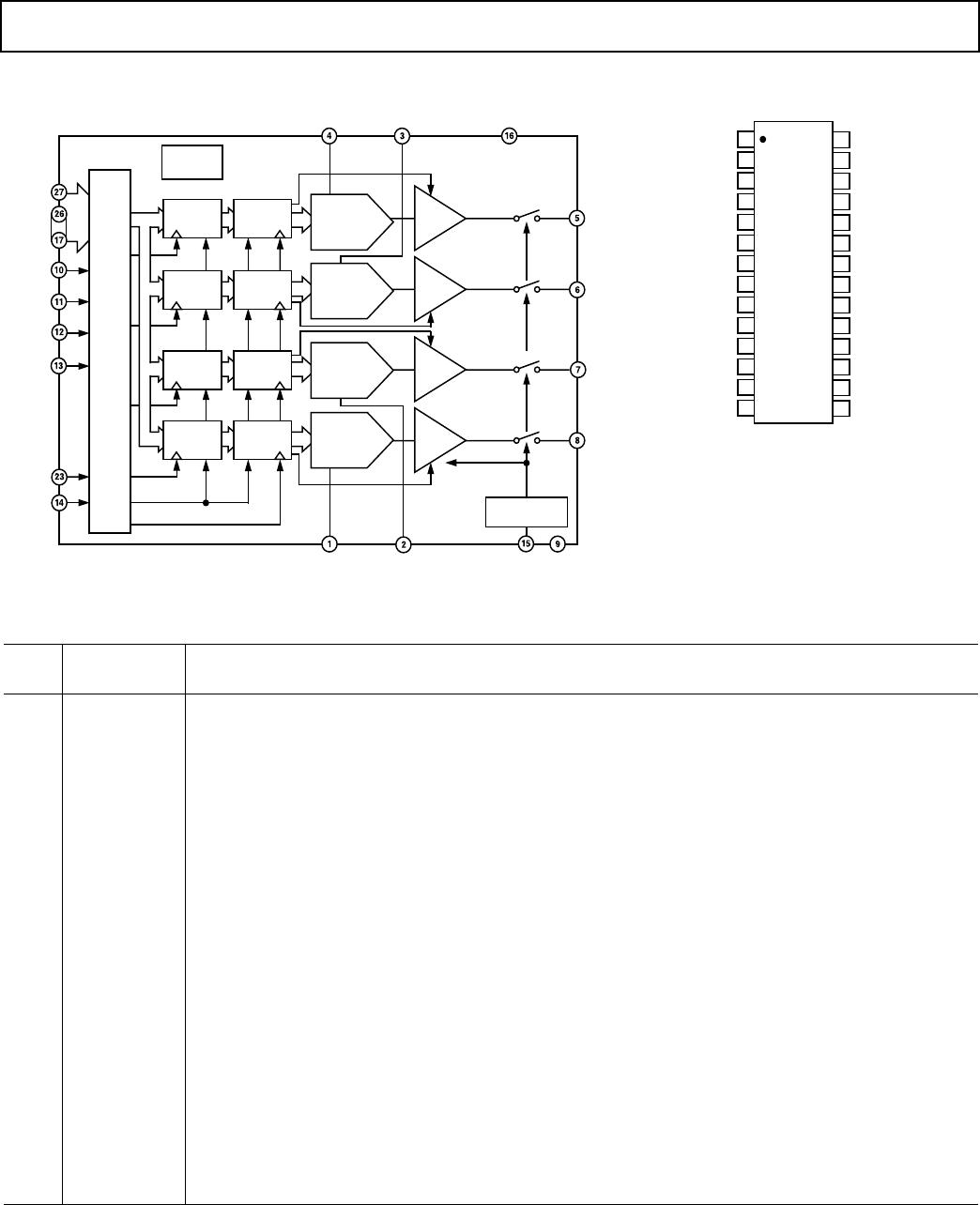
REV. 0
AD5334/AD5335/AD5336/AD5344
7
AD5336 FUNCTIONAL BLOCK DIAGRAM
V
OUT
A
BUFFER
GND
AD5336
V
OUT
B
BUFFER
V
OUT
C
BUFFER
V
OUT
D
BUFFER
POWER-ON
RESET
TO ALL DACS
AND BUFFERS
POWER-DOWN
LOGIC
PD
DAC
REGISTER
INPUT
REGISTER
V
REF
C
INTER-
FACE
LOGIC
V
DD
V
REF
B
GAIN
DB
9
DB
0
CS
WR
A0
A1
CLR
LDAC
.
.
.
V
REF
A
V
REF
D
RESET
INPUT
REGISTER
INPUT
REGISTER
INPUT
REGISTER
DAC
REGISTER
DAC
REGISTER
DAC
REGISTER
10-BIT
DAC
10-BIT
DAC
10-BIT
DAC
10-BIT
DAC
AD5336 PIN FUNCTION DESCRIPTIONS
Pin
No. Mnemonic Function
1V
REF
D Unbuffered Reference Input for DAC D.
2V
REF
C Unbuffered Reference Input for DAC C.
3V
REF
B Unbuffered Reference Input for DAC B.
4V
REF
A Unbuffered Reference Input for DAC A.
5V
OUT
A Output of DAC A. Buffered output with rail-to-rail operation.
6V
OUT
B Output of DAC B. Buffered output with rail-to-rail operation.
7V
OUT
C Output of DAC C. Buffered output with rail-to-rail operation.
8V
OUT
D Output of DAC D. Buffered output with rail-to-rail operation.
9 GND Ground Reference Point for All Circuitry on the Part.
10 CS Active Low Chip Select Input. This is used in conjunction with WR to write data to the parallel interface.
11 WR Active Low Write Input. This is used in conjunction with CS to write data to the parallel interface.
12 A0 LSB Address Pin for Selecting which DAC Is to Be Written to.
13 A1 MSB Address Pin for Selecting which DAC is to Be Written to.
14 LDAC Active Low Control Input that Updates the DAC Registers with the Contents of the Input Registers.
This allows all DAC outputs to be simultaneously updated.
15 PD Power-Down Pin. This active low control pin puts all DACs into power-down mode.
16 V
DD
Power Supply Pin. This part can operate from 2.5 V to 5.5 V and the supply should be decoupled with a
10 µF capacitor in parallel with a 0.1 µF capacitor to GND.
17–26 DB
0
–DB
9
10 Parallel Data Inputs. DB
9
is the MSB of these 10 bits.
27 GAIN Gain Control Pin. This controls whether the output range from the DAC is 0–V
REF
or 0–2 V
REF
.
28 CLR Asynchronous Active Low Control Input that Clears All Input Registers and DAC Registers to Zeros.
AD5336 PIN CONFIGURATION
TOP VIEW
(Not to Scale)
28
27
26
25
24
23
22
21
20
19
18
17
16
15
1
2
3
4
5
6
7
8
9
10
11
12
13
14
AD5336
LDAC
A1
A0
WR
CS
GND
V
OUT
D
V
REF
C
V
REF
B
V
REF
A
V
OUT
C
V
OUT
B
V
OUT
A
V
REF
D
PD
V
DD
DB
0
DB
1
DB
2
DB
3
DB
4
CLR
GAIN
DB
9
DB
8
DB
5
DB
6
DB
7
10-BIT
REV. 0
AD5334/AD5335/AD5336/AD5344
8
AD5344 FUNCTIONAL BLOCK DIAGRAM
V
OUT
A
BUFFER
GND
AD5344
V
OUT
B
BUFFER
V
OUT
C
BUFFER
V
OUT
D
BUFFER
POWER-ON
RESET
TO ALL DACS
AND BUFFERS
POWER-DOWN
LOGIC
PD
DAC
REGISTER
INPUT
REGISTER
V
REF
C
INTER-
FACE
LOGIC
V
DD
V
REF
B
CS
WR
A0
A1
LDAC
V
REF
A
V
REF
D
.
.
.
.
.
.
DB
11
DB
0
INPUT
REGISTER
INPUT
REGISTER
INPUT
REGISTER
DAC
REGISTER
DAC
REGISTER
DAC
REGISTER
12-BIT
DAC
12-BIT
DAC
12-BIT
DAC
12-BIT
DAC
AD5344 PIN FUNCTION DESCRIPTIONS
Pin
No. Mnemonic Function
1V
REF
D Unbuffered Reference Input for DAC D.
2V
REF
C Unbuffered Reference Input for DAC C.
3V
REF
B Unbuffered Reference Input for DAC B.
4V
REF
A Unbuffered Reference Input for DAC A.
5V
OUT
A Output of DAC A. Buffered output with rail-to-rail operation.
6V
OUT
B Output of DAC B. Buffered output with rail-to-rail operation.
7V
OUT
C Output of DAC C. Buffered output with rail-to-rail operation.
8V
OUT
D Output of DAC D. Buffered output with rail-to-rail operation.
9 GND Ground Reference Point for All Circuitry on the Part.
10 CS Active Low Chip Select Input. This is used in conjunction with WR to write data to the parallel interface.
11 WR Active Low Write Input. This is used in conjunction with CS to write data to the parallel interface.
12 A0 LSB Address Pin for Selecting which DAC Is to Be Written to.
13 A1 MSB Address Pin for Selecting which DAC Is to Be Written to.
14 LDAC Active Low Control Input that Updates the DAC Registers with the Contents of the Input Registers.
This allows all DAC outputs to be simultaneously updated.
15 PD Power-Down Pin. This active low control pin puts all DACs into power-down mode.
16 V
DD
Power Supply Pin. This part can operate from 2.5 V to 5.5 V and the supply should be decoupled with a
10 µF capacitor in parallel with a 0.1 µF capacitor to GND.
17–28 DB
0
–DB
11
12 Parallel Data Inputs. DB
11
is the MSB of these 12 bits.
AD5344 PIN CONFIGURATION
TOP VIEW
(Not to Scale)
28
27
26
25
24
23
22
21
20
19
18
17
16
15
1
2
3
4
5
6
7
8
9
10
11
12
13
14
AD5344
LDAC
A1
A0
WR
CS
GND
V
OUT
D
V
REF
C
V
REF
B
V
REF
A
V
OUT
C
V
OUT
B
V
OUT
A
V
REF
D
PD
V
DD
DB
0
DB
1
DB
2
DB
3
DB
4
DB
11
DB
10
DB
9
DB
8
DB
5
DB
6
DB
7
12-BIT
REV. 0
AD5334/AD5335/AD5336/AD5344
9
TERMINOLOGY
RELATIVE ACCURACY
For the DAC, Relative Accuracy or Integral Nonlinearity (INL)
is a measure of the maximum deviation, in LSBs, from a straight
line passing through the actual endpoints of the DAC transfer
function. Typical INL versus Code plot can be seen in Figures
5, 6, and 7.
DIFFERENTIAL NONLINEARITY
Differential Nonlinearity (DNL) is the difference between the
measured change and the ideal 1 LSB change between any two
adjacent codes. A specified differential nonlinearity of ± 1 LSB
maximum ensures monotonicity. This DAC is guaranteed mono-
tonic by design. Typical DNL versus Code plot can be seen in
Figures 8, 9, and 10.
OFFSET ERROR
This is a measure of the offset error of the DAC and the output
amplifier. It is expressed as a percentage of the full-scale range.
If the offset voltage is positive, the output voltage will still be
positive at zero input code. This is shown in Figure 3. Because
the DACs operate from a single supply, a negative offset cannot
appear at the output of the buffer amplifier. Instead, there will
be a code close to zero at which the amplifier output saturates
(amplifier footroom). Below this code there will be a deadband
over which the output voltage will not change. This is illustrated
in Figure 4.
GAIN ERROR
This is a measure of the span error of the DAC (including any
error in the gain of the buffer amplifier). It is the deviation in
slope of the actual DAC transfer characteristic from the ideal
expressed as a percentage of the full-scale range. This is illus-
trated in Figure 2.
OUTPUT
VOLTAGE
DAC CODE
POSITIVE
GAIN ERROR
NEGATIVE
GAIN ERROR
ACTUAL
IDEAL
Figure 2. Gain Error
OUTPUT
VOLTAGE
DAC CODE
POSITIVE
OFFSET
GAIN ERROR
AND
OFFSET
ERROR
ACTUAL
IDEAL
Figure 3. Positive Offset Error and Gain Error
Figure 4. Negative Offset Error and Gain Error

AD5336BRU

Mfr. #:
Manufacturer:
Analog Devices Inc.
Description:
Digital to Analog Converters - DAC Quad 10-Bit
Lifecycle:
New from this manufacturer.
Delivery:
DHL FedEx Ups TNT EMS
Payment:
T/T Paypal Visa MoneyGram Western Union