REV. 0
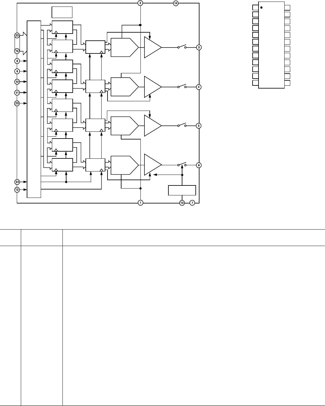
AD5334/AD5335/AD5336/AD5344
–4–
CAUTION
ESD (electrostatic discharge) sensitive device. Electrostatic charges as high as 4000 V readily
accumulate on the human body and test equipment and can discharge without detection. Although
the AD5334/AD5335/AD5336/AD5344 features proprietary ESD protection circuitry, permanent
damage may occur on devices subjected to high-energy electrostatic discharges. Therefore, proper
ESD precautions are recommended to avoid performance degradation or loss of functionality.
WARNING!
ESD SENSITIVE DEVICE
ABSOLUTE MAXIMUM RATINGS*
(T
A
= 25°C unless otherwise noted)
V
DD
to GND . . . . . . . . . . . . . . . . . . . . . . . . . . –0.3 V to +7 V
Digital Input Voltage to GND . . . . . . . .–0.3 V to V
DD
+ 0.3 V
Digital Output Voltage to GND . . . . . . –0.3 V to V
DD
+ 0.3 V
Reference Input Voltage to GND . . . . –0.3 V to V
DD
+ 0.3 V
V
OUT
to GND . . . . . . . . . . . . . . . . . . . –0.3 V to V
DD
+ 0.3 V
Operating Temperature Range
Industrial (B Version) . . . . . . . . . . . . . . . –40°C to +105°C
Storage Temperature Range . . . . . . . . . . . . –65°C to +150°C
Junction Temperature . . . . . . . . . . . . . . . . . . . . . . . . . . 150°C
TSSOP Package
Power Dissipation . . . . . . . . . . . . . . . (T
J
max – T
A
)/θ
JA
mW
θ
JA
Thermal Impedance (24-Lead TSSOP) . . . . . 128°C/W
θ
JA
Thermal Impedance (28-Lead TSSOP) . . . . . 97.9°C/W
θ
JC
Thermal Impedance (24-Lead TSSOP) . . . . . . 42°C/W
θ
JC
Thermal Impedance (28-Lead TSSOP) . . . . . . 14°C/W
Reflow Soldering
Peak Temperature . . . . . . . . . . . . . . . . . . . . . . 220 +5/–0°C
Time at Peak Temperature . . . . . . . . . . . . .10 sec to 40 sec
*Stresses above those listed under Absolute Maximum Ratings may cause perma-
nent damage to the device. This is a stress rating only; functional operation of the
device at these or any other conditions above those listed in the operational
sections of this specification is not implied. Exposure to absolute maximum rating
conditions for extended periods may affect device reliability.
ORDERING GUIDE
Model Temperature Range Package Description Package Option
AD5334BRU –40°C to +105°C TSSOP (Thin Shrink Small Outline Package) RU-24
AD5335BRU –40°C to +105°C TSSOP (Thin Shrink Small Outline Package) RU-24
AD5336BRU –40°C to +105°C TSSOP (Thin Shrink Small Outline Package) RU-28
AD5344BRU –40°C to +105°C TSSOP (Thin Shrink Small Outline Package) RU-28