Document Number: 001-65659 Rev. *I Page 13 of 26
CY7C65642
Upstream Port
D– 1 I/O/Z Upstream D– Signal.
D+ 2 I/O/Z Upstream D+ Signal.
Downstream Port 1
DD–[1] 3 I/O/Z Downstream D– Signal.
DD+[1] 4 I/O/Z Downstream D+ Signal.
OVR#[1] 25 I(R
UP
)
Overcurrent Condition Detection Input. Active LOW Overcurrent Condition
Detection Input. Only OVR#[1](pin 25) is enabled in Gang mode. OVR#[2](pin 24),
OVR#[3](pin 20) and OVR#[4](pin 19) are disabled in Gang mode.
Downstream Port 2
DD–[2] 6 I/O/Z Downstream D– Signal.
DD+[2] 7 I/O/Z Downstream D+ Signal.
OVR#[2] 24 I(R
UP
)
Overcurrent Condition Detection Input. Active LOW Overcurrent Condition
Detection Input. Only OVR#[1](pin 25) is enabled in Gang mode. This (OVR#[2]) pin
is disabled in Gang mode.
Downstream Port 3
DD–[3] 12 I/O/Z Downstream D– Signal.
DD+[3] 13 I/O/Z Downstream D+ Signal.
OVR#[3] 20 I(R
UP
)
Overcurrent Condition Detection Input. Active LOW Overcurrent Condition
Detection Input. Only OVR#[1](pin 25) is enabled in Gang mode. This (OVR#[3]) pin
is disabled in Gang mode.
Downstream Port 4
DD–[4] 15 I/O/Z Downstream D– Signal.
DD+[4] 16 I/O/Z Downstream D+ Signal.
OVR#[4] 19 I(R
UP
)
Overcurrent Condition Detection Input. Active LOW Overcurrent Condition
Detection Input. Only OVR#[1](pin 25) is enabled in Gang mode. This (OVR#[4]) pin
is disabled in Gang mode.
GND PAD P
Ground pin for the chip. It is the solderable exposed pad beneath the chip. Refer to
the Figure 4 on page 21.
Pin Definitions (continued)
28-pin QFN Package
Pin Name Pin No. Type
[3]
Description
Document Number: 001-65659 Rev. *I Page 14 of 26
CY7C65642
EEPROM Configuration Options
Systems using CY7C65642 have the option of using the default
descriptors to configure the hub. Otherwise, it must have an
external EEPROM for the device to have a unique VID, and PID.
The CY7C65642 can communicate with an SPI (microwire)
EEPROM like 93C46 or I
2
C EEPROM like 24C02. Example
EEPROM connections are shown as follows:
Note The 28-pin QFN package includes only support for I
2
C
EEPROM like ATMEL/24C02N_SU27 D, MICROCHIP/4LC028
SN0509, SEIKO/S24CS02AVH9. The 48-pin TQFP package
includes both I
2
C and SPI EEPROM connectivity options. In this
case, user can use either SPI or I
2
C connectivity at a time for
communicating to EEPROM. The 48-pin package supports
ATMEL/AT93C46DN-SH-T, in addition to the above mentioned
families. HX2VL can only read from SPI EEPROM. So field
programming of EEPROM will be supported only for I
2
C
EEPROM. The default VID and PID are 0x04B4 and 0x6572.
CY7C65642 verifies the check sum after power on reset and if
validated loads the configuration from the EEPROM. To prevent
this configuration from being overwritten, AMBER[1] is disabled
when the SPI EEPROM is present.
Byte 0: VID (LSB)
Least Significant Byte of Vendor ID
Byte 1: VID (MSB)
Most Significant Byte of Vendor ID
Byte 2: PID (LSB)
Least Significant Byte of Product ID
Byte 3: PID (MSB)]
Most Significant Byte of Product ID
Byte 4: ChkSum
CY7C65642 will ignore the EEPROM settings if ChkSum is
not equal to VID_LSB + VID_MSB + PID_LSB + PID_MSB +1
Byte 5: Reserved
Set to FEh
Byte 6: RemovablePorts
RemovablePorts[4:1] are the bits that indicate whether the
device attached to the corresponding downstream port is
removable (set to 0) or non-removable (set to 1). Bit 1
corresponds to Port 1, Bit 2 to Port 2 and so on. Default value
is 0 (removable). These bit values are reported appropriately
in the HubDescriptor:DeviceRemovable field.
Bits 0,5,6,7 are set to 0.
Byte 7: Port Number
Port Number indicates the number of downstream ports. The
values must be 1 to 4. Default value is 4.
Byte 8: Maximum Power
This value is reported in the Configuration Descriptor:
bMax-Power field and is the current in 2 mA increments that
is required from the upstream hubs. The allowed range is 00h
(0mA) to FAh(500mA). Default value is 32h (100mA)
Byte 9–15: Reserved
Set to FFh (except 11 which is FEh)
Byte 16: Vendor String Length
Length of the Vendor String
Byte 17–63: Vendor String
Value of Vendor String in ASCII code.
Byte 64: Product String Length
Length of the Product String
Byte 65–111: Product String
Value of Product String in ASCII code
Byte 112: Serial Number Length
Length of the Serial Number
Byte 113 onwards: Serial Number String
Serial Number String in ASCII code.
Byte Value
00h VID_LSB
01h VID_MSB
02h PID_LSB
03h PID_MSB
04h ChkSum
05h Reserved–FEh
06h Removable ports
07h Port number
08h Maximum power
09h–0Fh Reserved–FFh
10h Vendor string length
11h–3Fh Vendor string (ASCII code)
40h Product string length
CS
DI
SK
DO GND
NC2
NC1
VCC
AMBER[1]
AMBER[2]
GREEN[1]
GREEN[2]
VDD
AT93C46
A0
A2
A1
GND SDA
SCL
WP
VCC
TEST
AT24C02
VDD
PWR#[1]
I2C EEPROM Connection
SPI EEPROM Connection
41h–6Fh Product string (ASCII code)
70 h Serial number length
71h–80h Serial number string
Byte Value
Document Number: 001-65659 Rev. *I Page 15 of 26
CY7C65642
Pin Configuration Options
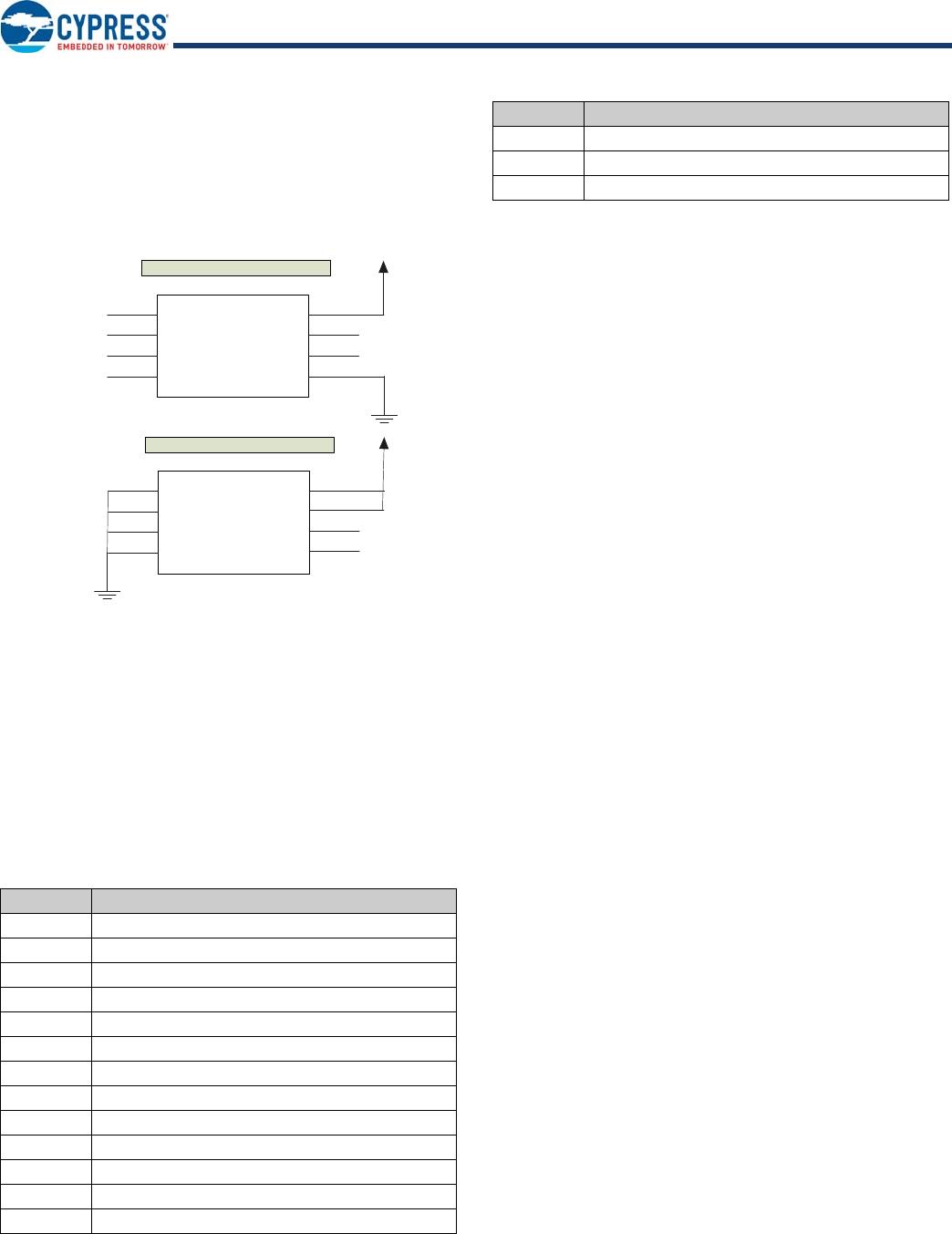
Power ON Reset
The power on reset can be triggered by external reset or internal
circuitry. The internal reset is initiated, when there is an unstable
power event for silicon’s internal core power (3.3 V ± 10%). The
internal reset is released 2.7 µs ± 1.2% after supply reaches
power good voltage (2.5 V to 2.8 V). The external reset pin,
continuously senses the voltage level (5 V) on the upstream
VBUS as shown in the figure. In the event of USB plug/unplug or
drop in voltage, the external reset is triggered. This reset trigger
can be configured using the resistors R1 and R2. Cypress
recommends that the reset time applied in external reset circuit
should be longer than that of the internal reset time.
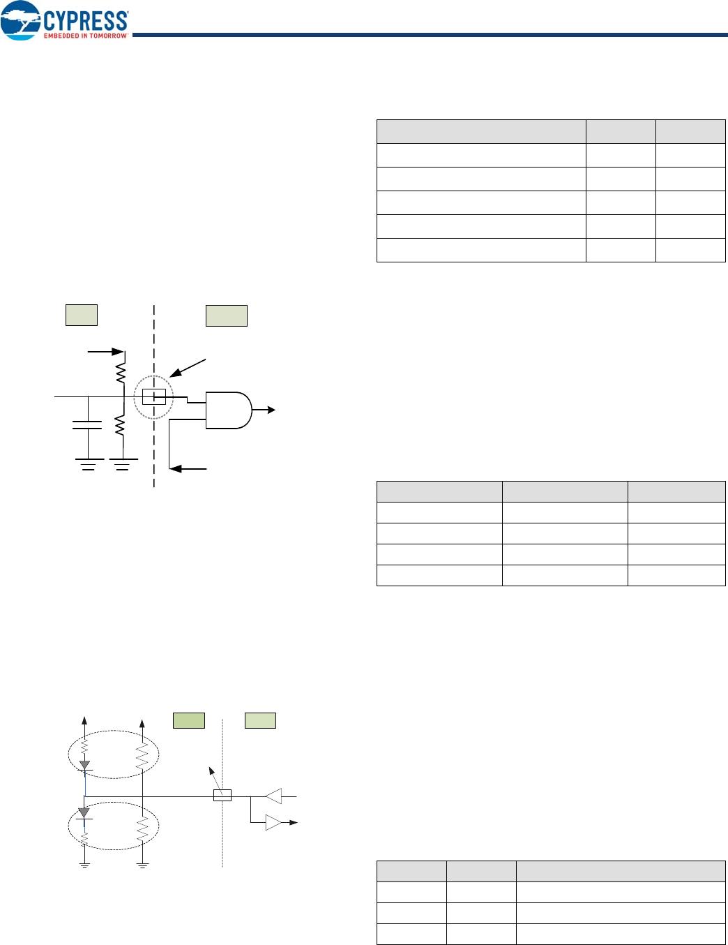
Gang/Individual Power Switching Mode
A single pin is used to set individual / gang mode as well as
output the suspend flag. This is done to reduce the pin count.
The individual or gang mode is decided within 20 µs after power
on reset. It has a setup time of 1ns. 50 to 60ms after reset, this
pin is changed to output mode. CY7C65642 outputs the suspend
flag, once it is globally suspended. Pull-down resistor of greater
than 100K is needed for Individual mode and a pull-up resistor
greater than 100K is needed for Gang mode. Figure below
shows the suspend LED indicator schematics. The polarity of
LED must be followed, otherwise the suspend current will be
over the spec limitation (2.5 mA).
Power Switch Enable Pin Polarity
The pin polarity is set active-high by pin-strapping the
PWR_PIN_POL pin to 1 and Active-Low by pin-strapping the
PWR_PIN_POL pin to 0. Thus, both kinds of power switches
are supported. This feature is not supported in 28-pin QFN
package.
Port Number Configuration
In addition to the EEPROM configuration, as described
above, configuring the hub for 2/3/4 ports is also supported
using pin-strapping SET_PORT_NUM1 and
SET_PORT_NUM2, as shown in following table.Pin strapping
option is not supported in the 28-pin QFN package.
Non Removable Ports Configuration
In embedded systems, downstream ports that are always
connected inside the system, can be set as non-removable
(always connected) ports, by pin-strapping the corresponding
FIXED_PORT# pins 1~4 to High, before power on reset. At POR,
if the pin is pull high, the corresponding port is set to
non-removable. This is not supported in the 28-pin QFN
package.
Reference Clock Configuration
This hub can support, optional 27/48-MHz clock source. When
on-board 27/48-MHz clock is present, then using this feature,
system integrator can further reduce the BOM cost by eliminating
the external crystal. This is available through GPIO pin
configuration shown below. This is not supported in the 28-pin
QFN package.
Global
Reset#
Int. 3.3V power-good
detection circuit input
(USB PHY reset)
Ext. VBUS power-good
detection circuit input
(Pin"RESET#")
VBUS
(External 5V)
R1
R2
INT
EXT
PCB
Silicon
0 : INDIVIDUAL MODE
1: GANG MODE
SUSPEND OUT
VDD (3.3V)
SUSPEND
INDICATOR
VDD (3.3V)
100K
100K
GANG/SUSPEND
SiliconPCB
GANG MODE
INDIVIDUAL MODE
Table 1. Features supported in 48-pin and 28-pin packages
Supported Features 48-pin 28-pin
Port number configuration Yes No
Non-removable port configuration Yes No
Reference clock configuration Yes No
Power switch enable polarity Yes No
LED Indicator Yes No
SET_PORT_NUM2 SET_PORT_NUM1 # Ports
1 1 1 (Port 1)
1 0 2 (Port 1/2)
0 1 3 (Port 1/2/3)
0 0 4 (All ports)
SEL48 SEL27 Clock Source
0 1 48-MHz OSC-in
1 0 27-MHz OSC-in
1 1 12-MHz X’tal/OSC-in

CY7C65642-28LTXC

Mfr. #:
Manufacturer:
Cypress Semiconductor
Description:
USB Interface IC TetraHub Ctrl USB2.0
Lifecycle:
New from this manufacturer.
Delivery:
DHL FedEx Ups TNT EMS
Payment:
T/T Paypal Visa MoneyGram Western Union