Document Number: 001-65659 Rev. *I Page 24 of 26
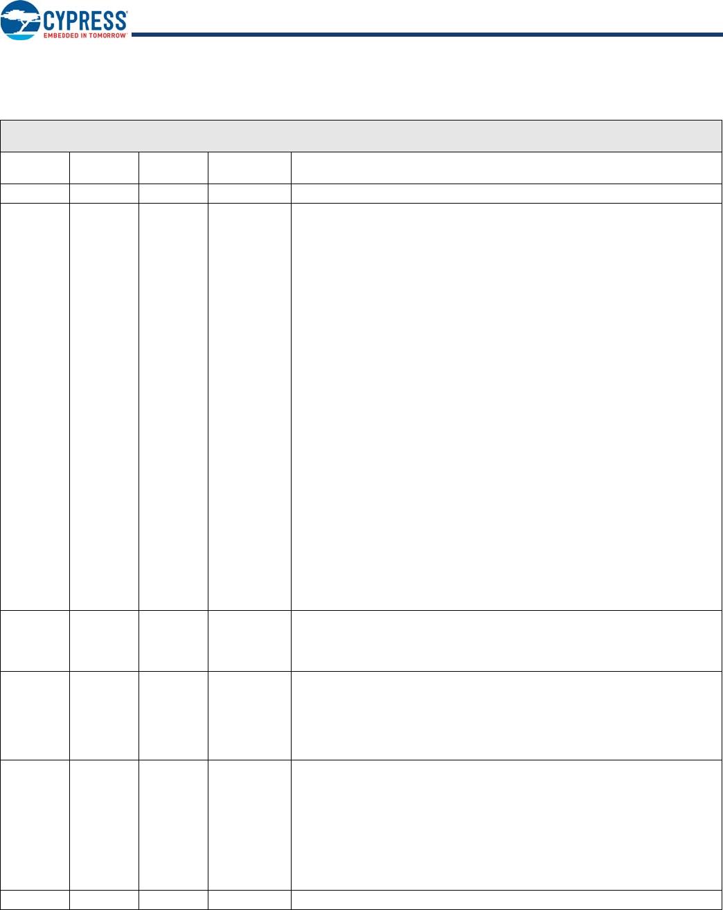
Document History Page
Document Title: CY7C65642, HX2VL – Very Low Power USB 2.0 TetraHub™ Controller
Document Number: 001-65659
Rev. ECN
Orig. of
Change
Submission
Date
Description of Change
** 3176751 SWAK 02/18/2011 New data sheet.
*A 3250883
SWAK /
AASI
06/29/2011
Updated Functional Overview (Updated Port Indicators (Added a Note
“Pin-strapping GREEN#[1] and GREEN#[2] enables proprietary function that
may affect the normal functionality of HX2VL. Configuring Port #1 and #2 as
non-removable by pin-strapping should be avoided.”).
Updated Pin Configurations (Updated Figure 1 (Pin of the 48-pin TQFP
package was named SELF_PWR. It is changed to SELFPWR.)).
Updated Pin Definitions (Updated description of XIN pin to “12-MHz crystal
clock input, or 12-MHz clock input” (since 28-pin package does not support 27
and 48 MHz), updated description of XOUT pin to “12-MHz Crystal OUT. (NC
if external clock is used)”, changed value from 680
to 650
RREF pinOVR# pins
from “Default is Active LOW” to “Active LOW Overcurrent Condition Detection
Input” (since the polarity is not configurable), changed all seven occurrences
of “Refer “48-pin TQFP Pin Configuration” on page 5” to “Refer Pin
Configuration Options on page 15”, added Note 2 and referred the same Note
in GREEN#[1] and GREEN#[2] pins).
Updated Pin Definitions (Updated description of XIN pin to “12-MHz crystal
clock input, or 12-MHz clock input” (since 28-pin package does not support 27
and 48 MHz), updated description of XOUT pin to “12-MHz Crystal OUT. (NC
if external clock is used)”,
OVR# pins from
“Default is Active LOW” to “Active LOW Overcurrent Condition Detection Input”
(since the polarity is not configurable)).
Updated Functional Overview (Updated Power Regulator (Changed regulator’s
maximum current loading from 200 mA to 150 mA)).
Updated Pin Configuration Options (Updated Power Switch Enable Pin Polarity
(Replaced first two occurrences of the word “setting” with “pin-strapping”)).
Updated Electrical Characteristics (Updated DC Electrical Characteristics
(Updated maximum value of I
SUSP
parameter to 903 µA, updated maximum
values of I
CC
parameter)).
*B 3327505 AASI 07/27/2011
Changed status from Preliminary to Final.
Updated Pin Definitions (Minor edits).
Updated Ordering Information (Updated part numbers) and Ordering Code
Definitions.
*C 3525169 AASI 02/16/2012
Updated Pin Configurations (Updated Figure 1 (Renamed SPI_DI to
SPI_MOSI, renamed SPI_DO to SPI_MISO respectively for clarity)).
Updated Pin Definitions (Renamed SPI_DI to SPI_MOSI, renamed SPI_DO to
SPI_MISO respectively for clarity).
Updated Pin Definitions (Updated description of PWR# of 28-pin package (To
describe the alternate function I2C_SDA)).
*D 3637477 AASI 07/02/2012
Updated EEPROM Configuration Options (Changed the value of Byte 5 to FEh
to match with the tabular column).
Updated Electrical Characteristics (Updated DC Electrical Characteristics
(Splitted the Max column into two columns namely External regulator and
Internal regulator for I
SUSP
and I
CC
parameters and updated the corresponding
values)).
Added Thermal Resistance.
Updated Ordering Information (Updated part numbers).
Updated to new template.
*E 3995708 PRJI 05/09/2013 Added Silicon Errata for the HX2VL, CY7C65642 Product Family.