AD7873 Data Sheet
Rev. F | Page 12 of 28
Figure 23. AC PSRR vs. Supply Ripple Frequency
Figure 23 shows the power supply rejection ratio vs. V
DD
supply
frequency for the AD7873. The power supply rejection ratio is
defined as the ratio of the power in the ADC output at full-scale
frequency, f, to the power of a 100 mV sine wave applied to the
ADC V
CC
supply of frequency f
S
PSSR (dB) = 10log(Pf/Pf
s
)
where:
Pf is power at frequency, f, in ADC output.
Pf
s
is power at frequency, f
s
, coupled onto the ADC V
CC
supply.
Here a 100 mV p-p sine wave is coupled onto the V
CC
supply.
Decoupling capacitors of 10 µF and 0.1 µF were used on the supply.
–120
–100
–80
–60
–40
–20
0
PSRR (dB)
0 10 20 30 40 50 60 70 80 90 100
V
CC
RIPPLE FREQUENCY (kHz)
V
CC
= 3V
100mV p-p SINE WAVE ON +V
CC
V
REF
= 2.5V EXT REFERENCE
f
SAMPLE
= 125kHz,
f
IN
= 20kHz
02164-023
Data Sheet AD7873
Rev. F | Page 13 of 28
CIRCUIT INFORMATION
The AD7873 is a fast, low power, 12-bit, single-supply analog-
to-digital converter (ADC). The AD7873 can be operated from
a 2.2 V to 5.25 V supply. When operated from either a 5 V
supply or a 3 V supply, the AD7873 is capable of throughput
rates of 125 kSPS when provided with a 2 MHz clock.
The AD7873 provides the user with on-chip track-and-hold,
multiplexer, ADC, reference, temperature sensor, and serial
interface, housed in a tiny 16-lead QSOP, TSSOP, or LFCSP
package, offering the user considerable space-saving advantages
over alternative solutions. The serial clock input (DCLK)
accesses data from the part and also provides the clock source
for the successive approximation ADC. The analog input range
is 0 V to V
REF
(where the externally applied V
REF
can be between
1 V and +V
CC
). The AD7873 has a 2.5 V reference on-board
with this reference voltage available for use externally if buffered.
The analog input to the ADC is provided via an on-chip
multiplexer. This analog input can be any one of the X, Y, and Z
panel coordinates, the battery voltage, or the chip temperature.
The multiplexer is configured with low resistance switches that
allow an unselected ADC input channel to provide power and
an accompanying pin to provide ground for an external device.
For some measurements, the on resistance of the switches could
present a source of error. However, with a differential input to
the converter and a differential reference architecture, this error
can be negated.
ADC TRANSFER FUNCTION
The output coding of the AD7873 is straight binary. The
designed code transitions occur at successive integer LSB values
(that is, 1 LSB, 2 LSBs, and so on). The LSB size is V
REF
/4096.
The ideal transfer characteristic for the AD7873 is shown in
Figure 24.
Figure 24. Transfer Characteristic
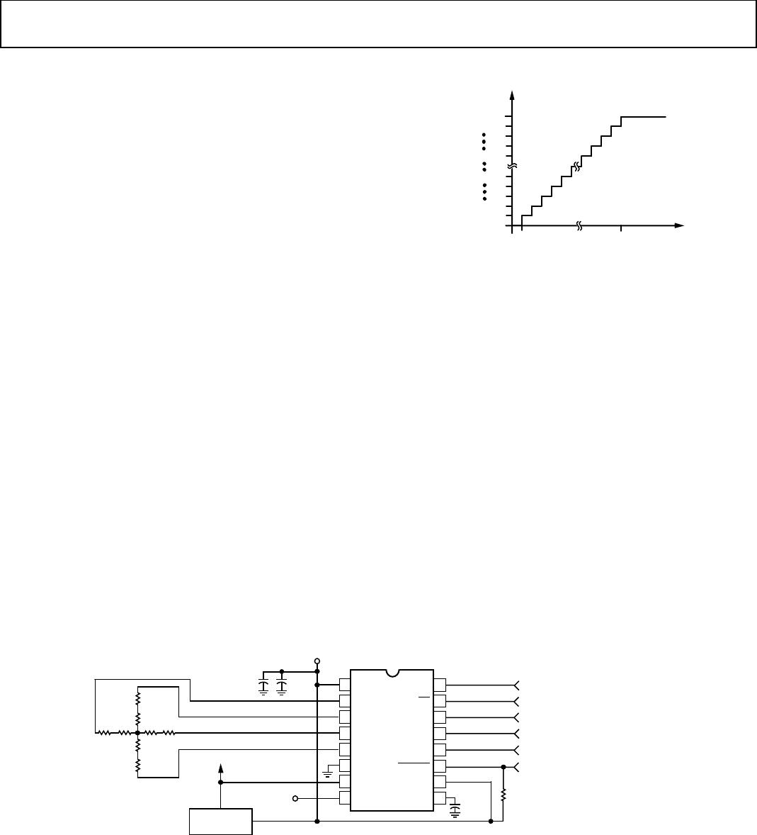
TYPICAL CONNECTION DIAGRAM
Figure 25 shows a typical connection diagram for the AD7873
in a touch screen control application. The AD7873 features an
internal reference, but this can be overdriven with an external
low impedance source between 1 V and +V
CC
. The value of the
reference voltage sets the input range of the converter. The
conversion result is output MSB first, followed by the remaining
11 bits and three trailing zeros, depending on the number of
clocks used per conversion (see the Serial Interface section). For
applications where power consumption is a concern, the power
management option should be used to improve power perform-
ance. See Table 8 for available power management options.
Figure 25. Typical Application Circuit
ADC CODE
ANALOG INPUT
1LSB
0V
+V
REF
– 1LSB
1LSB = V
REF
/4096
111...111
111...110
111...000
011...111
000...010
000...001
000...000
02164-024
16
15
14
13
12
11
9
8
1
2
3
4
7
6
5
10
TOUCH
SCREEN
1µF TO 10µF
(OPTIONAL)
2.2V TO 5V
0.1µF
0.1µF
AUXILIARY
INPUT
AD7873
+V
CC
X+
Y+
X–
Y–
GND
V
BAT
AUX
DCLK
CS
DIN
BUSY
DOUT
PENIRQ
+V
CC
V
REF
SERIAL/CONVERSION CLOCK
CHIP SELECT
SERIAL DATA IN
CONVERTER STATUS
SERIAL DATA OUT
PEN INTERRUPT
50k
TO BATTERY
VOLTAGE
REGULATOR
+ +
+
02164-025
AD7873 Data Sheet
Rev. F | Page 14 of 28
ANALOG INPUT
Figure 26 shows an equivalent circuit of the analog input
structure of the AD7873 that contains a block diagram of the
input multiplexer, the differential input of the ADC, and the
differential reference.
Table 6 shows the multiplexer address corresponding to each
analog input, both for the SER/
DFR
bit in the control register
set high and low. The control bits are provided serially to the
device via the DIN pin. For more information on the control
register, see the Control Register section.
When the converter enters hold mode, the voltage difference
between the +IN and IN inputs (see Figure 26) is captured on
the internal capacitor array. The input current on the analog
inputs depends on the conversion rate of the device. During the
sample period, the source must charge the internal sampling
capacitor (typically 37 pF). Once the capacitor is fully charged,
there is no further input current. The rate of charge transfer
from the analog source to the converter is a function of
conversion rate.
Figure 26. Equivalent Analog Input Circuit
Table 6. Analog Input, Reference, and Touch Screen Control
A2 A1 A0
SER/
DFR
Analog Input X Switches Y Switches +REF
1
REF
1
0 0 0 1 TEMP0 Off Off V
REF
GND
0 0 1 1 X+ Off On V
REF
GND
0 1 0 1 VBAT Off Off V
REF
GND
0 1 1 1 X+ (Z1) X+ Off Y+ On V
REF
GND
X– On Y– Off
1
0
0
1
Y– (Z2)
X+ Off
Y+ On
V
REF
GND
X– On Y– Off
1 0 1 1 Y+ On Off V
REF
GND
1 1 0 1 AUX Off Off V
REF
GND
1 1 1 1 TEMP1 Off Off V
REF
GND
0 0 0 0
Invalid Address. Test Mode: Switches out the TEMP0 diode to the
PENIRQ
pin.
0 0 1 0 X+ Off On Y+ Y–
0
1
0
0
Invalid Address
0 1 1 0 X+ (Z1) X+ Off Y+ On Y+ X–
X– On Y– Off
1 0 0 0 Y– (Z2) X+ Off Y+ On Y+ X–
X– On Y– Off
1 0 1 0 Y+ ON Off X+ X–
1 1 0 0
Outputs Identity Code, 1000 0000 0000.
1
1
1
0
Invalid address. Test mode: Switches out the TEMP1 diode to the
PENIRQ
pin.
1
Internal node, not directly accessible by the user.
X+ Y+
REF
INT/
EXT
X– Y– GND
6-TO-1
MUX
3-TO-1
MUX
3-TO-1
MUX
IN+
IN+
IN– REF–
REF+
ADC CORE DATA OUT
V
CC
Y–
Y+
X+
X–
ON-CHIP SWITCHES
X+
Y+
Y–
V
BAT
AUX
TEMP
02164-026

AD7873BRQZ-REEL

Mfr. #:
Manufacturer:
Analog Devices Inc.
Description:
Touch Screen Controllers 27V 12-BIT TouchScrn Digitizer
Lifecycle:
New from this manufacturer.
Delivery:
DHL FedEx Ups TNT EMS
Payment:
T/T Paypal Visa MoneyGram Western Union