Data Sheet AD7873
Rev. F | Page 3 of 28
SPECIFICATIONS
V
CC
= 2.7 V to 3.6 V, V
REF
= 2.5 V internal or external, f
DCLK
= 2 MHz; T
A
= 40°C to +85°C, unless otherwise noted.
Table 1.
Parameter AD7873A
1
AD7873B
1
Unit Test Conditions/Comments
DC ACCURACY
Resolution 12 12 Bits
No Missing Codes 11 12 Bits min
Integral Nonlinearity
2
±2 ± 1 LSB max
Differential Nonlinearity
2
–0.9/+1.5 LSB max
Offset Error
2
±6 ±6 LSB max +V
CC
= 2.7 V
Gain Error
2
±4 ±4 LSB max External reference
Noise 70 70 µV rms typ
Power Supply Rejection 70 70 dB typ
On Resistance
2
Y+, X+ 5 5 Ω typ
Y–, X 6 6 Ω typ
ANALOG INPUT
Input Voltage Ranges 0 to V
REF
0 to V
REF
V
DC Leakage Current ±0.1 ±0.1 µA typ
Input Capacitance 37 37 pF typ
REFERENCE INPUT/OUTPUT
Internal Reference Voltage 2.45/2.55 2.45/2.55 V min/max
Internal Reference Tempco ±15 ±15 ppm/°C typ
V
REF
Input Voltage Range 1/V
CC
1/V
CC
V min/max
DC Leakage Current ±1 ± 1 µA max
V
REF
Input Impedance 1 1 typ
CS = GND or +V
CC
; typically 260 Ω when the
on-board reference is enabled
TEMPERATURE MEASUREMENT
Temperature Range –40/+85 –40/+85 °C min/max
Resolution
Differential Method
3
1.6 1.6 °C typ
Single Conversion Method
4
0.3 0.3 °C typ
Accuracy
Differential Method
3
±2 ±2 °C typ
Single Conversion Method
4
±2 ±2 °C typ
BATTERY MONITOR
Input Voltage Range 0/6 0/6 V min/max
Input Impedance 10 10 typ Sampling; 1 GΩ when battery monitor is off
Accuracy ±2.5 ±2 % max External reference
±3 ±3 % max Internal reference
LOGIC INPUTS
Input High Voltage, V
INH
2.4 2.4 V min
Input Low Voltage, V
INL
0.4 0.4 V max
IN
±1
±1
µA max
Typically 10 nA, V
IN
= 0 V or +V
CC
Input Capacitance, C
IN
5
10 10 pF max
AD7873 Data Sheet
Rev. F | Page 4 of 28
Parameter AD7873A
1
AD7873B
1
Unit Test Conditions/Comments
LOGIC OUTPUTS
Output High Voltage, V
OH
V
CC
– 0.2 V
CC
– 0.2 V min I
SOURCE
= 250 µA; V
CC
= 2.2 V to 5.25 V
Output Low Voltage, V
OL
0.4 0.4 V max I
SINK
= 250 µA
PENIRQ Output Low Voltage, V
OL
0.4 0.4 V max 100 kΩ pull-up; I
SINK
= 250 µA
Floating-State Leakage Current ±10 ±10 µA max
Floating-State Output Capacitance
5
10 10 pF max
Output Coding Straight (Natural) Binary
CONVERSION RATE
Conversion Time 12 12 DCLK cycles max
Track-and-Hold Acquisition Time 3 3 DCLK cycles min
125
125
kSPS max
POWER REQUIREMENTS
+V
CC
(Specified Performance) 2.7/3.6 2.7/3.6 V min/max Functional from 2.2 V to 5.25 V
CC
6
Digital I/Ps = 0 V or V
CC
Normal Mode (f
SAMPLE
= 125 kSPS) 380 380 µA max Internal reference off, V
CC
= 3.6 V, 240 µA typ
670 670 µA typ Internal reference on, V
CC
= 3.6 V
Normal Mode (f
SAMPLE
= 12.5 kSPS) 170 170 µA typ Internal reference off, V
CC
= 2.7 V, f
DCLK
= 200 kHz
Normal Mode (Static) 150 150 µA typ Internal reference off, V
CC
= 3.6 V
580 580 µA typ Internal reference on, V
CC
= 3.6 V
Shutdown Mode (Static) 1 1 µA max 200 nA typ
Power Dissipation
6
Normal Mode (f
SAMPLE
= 125 kSPS) 1.368 1.368 mW max Internal reference off, V
CC
= 3.6 V
2.412 2.412 mW typ Internal reference on, V
CC
= 3.6 V
Shutdown 3.6 3.6 µW max V
CC
= 3.6 V
1
Temperature range as follows: A, B Versions: 40°C to +85°C.
2
See the Terminology section.
3
Difference between TEMP0 and TEMP1 measurement. No calibration necessary.
4
Temperature drift is 2.1 mV/°C.
5
Sample tested @ 25°C to ensure compliance.
6
See the Power vs. Throughput Rate section.
Data Sheet AD7873
Rev. F | Page 5 of 28
TIMING SPECIFICATIONS
T
A
= T
MIN
to T
MAX
, unless otherwise noted; V
CC
= 2.7 V to 5.25 V, V
REF
= 2.5 V.
Table 2. Timing Specifications
1
Parameter Limit at T
MIN
, T
MAX
Unit Description
f
DCLK
2
10 kHz min
2 MHz max
t
ACQ
1.5 µs min Acquisition time
t
1
10 ns min
CS falling edge to first DCLK rising edge
t
2
60 ns max
CS falling edge to busy three-state disabled
t
3
3
60 ns max
CS falling edge to DOUT three-state disabled
t
4
200 ns min DCLK high pulse width
t
5
200 ns min DCLK low pulse width
t
6
60 ns max DCLK falling edge to BUSY rising edge
t
7
10 ns min Data setup time prior to DCLK rising edge
t
8
10 ns min Data valid to DCLK hold time
t
9
3
200 ns max Data access time after DCLK falling edge
t
10
0 ns min
CS rising edge to DCLK ignored
t
11
100 ns max
CS rising edge to BUSY high impedance
t
12
4
100 ns max
CS rising edge to DOUT high impedance
1
Sample tested at 25°C to ensure compliance. All input signals are specified with tr = tf = 5 ns (10% to 90% of V
CC
) and timed from a voltage level of 1.6 V.
2
Mark/space ratio for the DCLK input is 40/60 to 60/40.
3
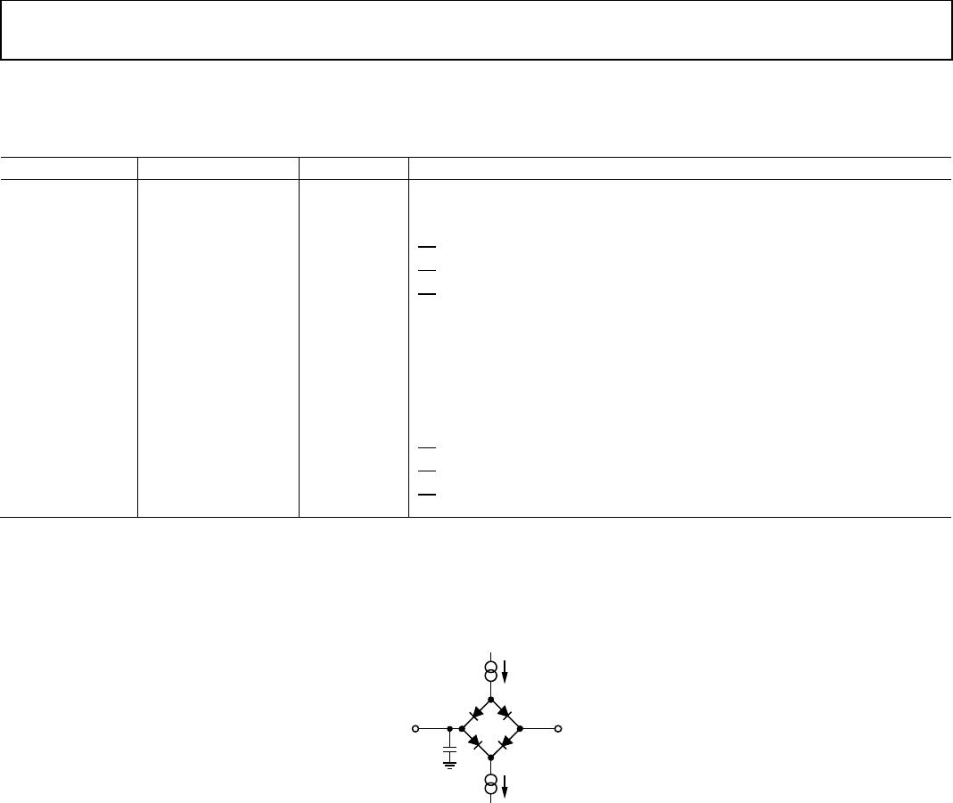
Measured with the load circuit of Figure 2 and defined as the time required for the output to cross 0.4 V or 2.0 V.
4
t
12
is derived from the measured time taken by the data outputs to change 0.5 V when loaded with the circuit of Figure 2. The measured number is then extrapolated
back to remove the effects of charging or discharging the 50 pF capacitor. This means that the time, t
12
, quoted in the timing characteristics is the true bus relinquish
time of the part and is independent of the bus loading.
Figure 2. Load Circuit for Digital Output Timing Specifications
200µA I
OL
200µA I
OH
1.6V
TO OUTPUT
PIN
C
L
50pF
02164-002

AD7873BRQZ-REEL

Mfr. #:
Manufacturer:
Analog Devices Inc.
Description:
Touch Screen Controllers 27V 12-BIT TouchScrn Digitizer
Lifecycle:
New from this manufacturer.
Delivery:
DHL FedEx Ups TNT EMS
Payment:
T/T Paypal Visa MoneyGram Western Union