Data Sheet AD7873
Rev. F | Page 15 of 28
Acquisition Time
The track-and-hold amplifier enters tracking mode on the
falling edge of the fifth DCLK after the start bit is detected (see
Figure 35). The time required for the track-and-hold amplifier
to acquire an input signal depends on how quickly the 37 pF
input capacitance is charged. With zero source impedance on
the analog input, three DCLK cycles are always sufficient to
acquire the signal to the 12-bit level. With a source impedance
(R
IN
) on the analog input, the actual acquisition time required is
calculated using the formula:
( )
pF37Ω1004.8 ×+×=
IN
ACQ
Rt
where R
IN
is the source impedance of the input signal, and 100 Ω,
37 pF is the input RC. Depending on the frequency of DCLK
used, three DCLK cycles may or may not be sufficient to acquire
the analog input signal with various source impedance values.
Touch Screen Settling
In some applications, external capacitors could be required
across the touch screen to filter noise associated with it, for
example, noise generated by the LCD panel or backlight
circuitry. The value of these capacitors causes a settling time
requirement when the panel is touched. The settling time
typically appears as a gain error. There are several methods for
minimizing or eliminating this issue. The problem can be that
the input signal, reference, or both, have not settled to their
final value before the sampling instant of the ADC. Additionally,
the reference voltage could still be changing during the conversion
cycle. One option is to stop or slow down the DCLK for the
required touch screen settling time. This allows the input and
reference to stabilize for the acquisition time, resolving the issue
for both single-ended and differential modes.
The other option is to operate the AD7873 in differential mode
only for the touch screen, and program the AD7873 to keep
the touch screen drivers on and not go into power-down
(PD0 = PD1 = 1). Several conversions could be required,
depending on the settling time required and the AD7873 data
rate. Once the required number of conversions have been made,
the AD7873 can then be placed in a power-down state on the
last measurement. The last method is to use the 15-DCLK cycle
mode, maintaining the touch screen drivers on until it is
commanded by the processor to stop.
Internal Reference
The AD7873 has an internal reference voltage of 2.5 V. The
internal reference is available on the V
REF
pin for external use in
the system; however, it must be buffered before it is applied
elsewhere. The on-chip reference can be turned on or off with
the power-down address, PD1 = 1 (see Table 8 and Figure 27).
Typically, the reference voltage is only used in single-ended
mode for battery monitoring, temperature measurement, and
for using the auxiliary input. Optimal touch screen performance
is achieved when using the differential mode. The power-up
time of the 2.5 V reference is typically 10 µs without a load;
however, a 0.1 µF capacitor on the V
REF
pin is recommended for
optimum performance because it affects the power-up time (see
Figure 20).
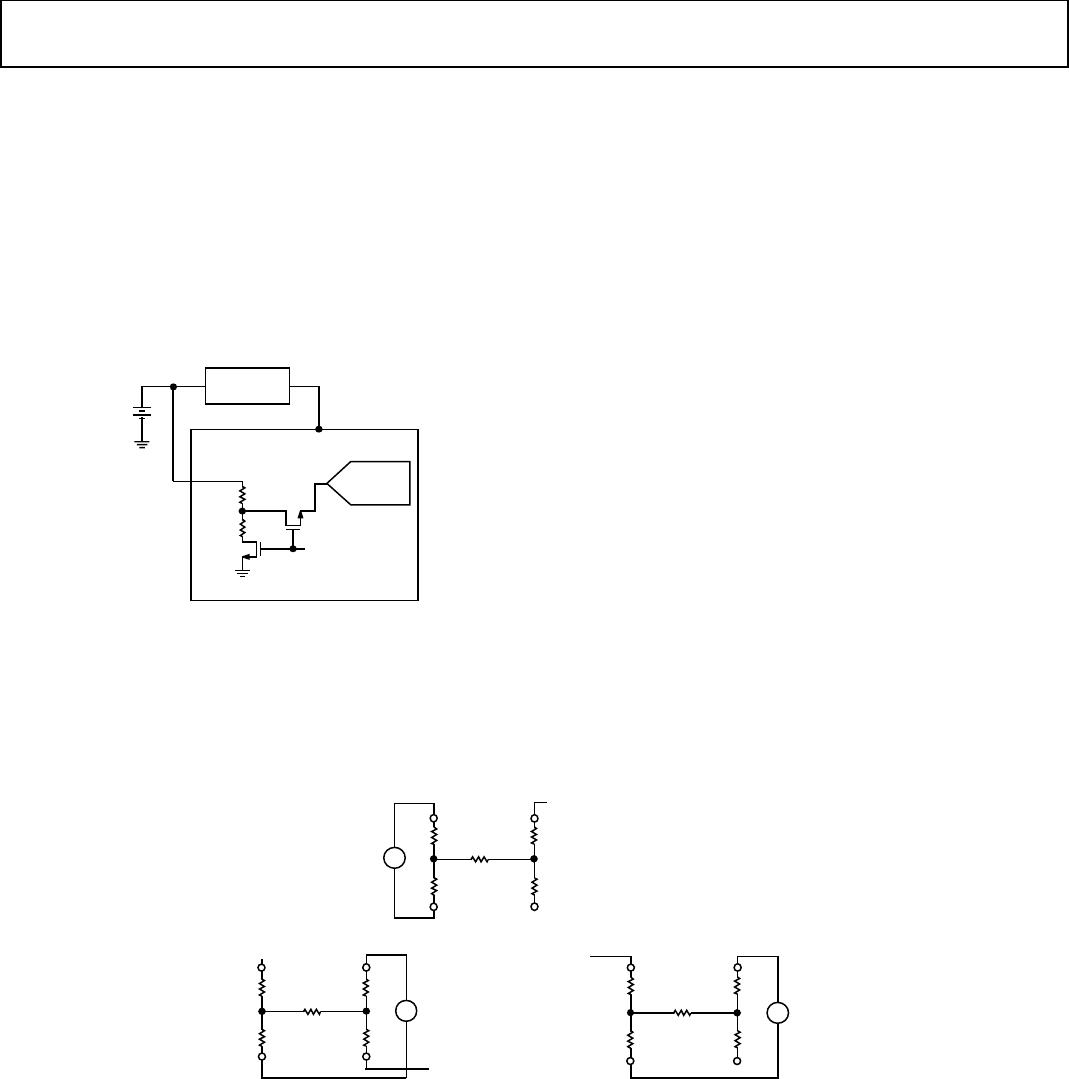
Figure 27. On-Chip Reference Circuitry
Reference Input
The voltage difference between +REF and −REF (see Figure 26)
sets the analog input range. The AD7873 operates with a refer-
ence input in the range of 1 V to +V
CC
. Figure 27 shows the
on-chip reference circuitry on the AD7873. The internal
reference on the AD7873 can be overdriven with an external
reference; for best performance, however, the internal reference
should be disabled when an external reference is applied,
because SW1 in Figure 27 opens on the AD7873 when the
internal reference is disabled. The on-chip reference always is
available at the V
REF
pin as long as the reference is enabled. The
input impedance seen at the V
REF
pin is approximately 260
when the internal reference is enabled. When it is disabled, the
input impedance seen at the V
REF
pin is in the region.
When making touch screen measurements, conversions can be
made in differential (ratiometric) mode or single-ended mode.
If the SER/
DFR
bit is set to 1 in the control register, then a
single-ended conversion is performed. Figure 28 shows the
configuration for a single-ended Y coordinate measurement.
The X+ input is connected to the analog-to-digital converter,
the Y+ and Ydrivers are turned on, and the voltage on X+ is
digitized. The conversion is performed with the ADC referenced
from GND to V
REF
. This V
REF
is either the on-chip reference or
the voltage applied at the V
REF
pin externally, and is determined
by the setting of the power management Bit PD0 and Bit PD1
(see Table 7). The advantage of this mode is that the switches
that supply the external touch screen can be turned off once the
acquisition is complete, resulting in a power savings. However,
the on resistance of the Y drivers affects the input voltage that
can be acquired. The full touch screen resistance could be in the
order of 200 Ω to 900 Ω, depending on the manufacturer. Thus,
if the on resistance of the switches is approximately 6 Ω, true
full-scale and zero-scale voltages cannot be acquired, regardless
of where the pen/stylus is on the touch screen. Note that the
minimum touch screen resistance recommended for use with
X+
Y+
V
REF
260
SW1
3-TO-1
MUX
2.5V
REF
ADC
BUF
02164-027
AD7873 Data Sheet
Rev. F | Page 16 of 28
the AD7873 is approximately 70 Ω. In this mode of operation,
therefore, some voltage is likely to be lost across the internal
switches, and it is unlikely that the internal switch resistance
will track the resistance of the touch screen over temperature
and supply, providing an additional source of error.
Figure 28. Single-Ended Reference Mode (SER/
DFR
= 1)
The alternative to this situation is to set the SER/
DFR
bit low.
Again, making a Y coordinate measurement is considered, but
now the +REF and REF nodes of the ADC are connected
directly to the Y+ and Ypins. This means the analog-to-digital
conversion is ratiometric. The result of the conversion is always
a percentage of the external resistance, independent of how it
could change with respect to the on resistance of the internal
switches. Figure 29 shows the configuration for a ratiometric
Y coordinate measurement.
Figure 29. Differential Reference Mode (SER/
DFR
= 0)
The disadvantage of this mode of operation is that during both
the acquisition phase and conversion process, the external
touch screen must remain powered. This results in additional
supply current for the duration of the conversion.
MEASUREMENTS
Temperature Measurement
Two temperature measurement options are available on the
AD7873, the single conversion method and the differential
conversion method. Both methods are based on an on-chip
diode measurement.
In the single conversion method, a diode voltage is digitized
and recorded at a fixed calibration temperature. Any subsequent
polling of the diode provides an estimate of the ambient tempera-
ture through extrapolation from the calibration temperature
diode result. This assumes a diode temperature drift of
approximately 2.1 mV/°C. This method provides a resolution
of approximately 0.3°C and a predicted accuracy of ±3°C.
The differential conversion method is a two-point measurement.
The first measurement is performed with a fixed bias current
into a diode, and the second measurement is performed with a
fixed multiple of the bias current into the same diode. The
voltage difference in the diode readings is proportional to
absolute temperature and is given by the following formula:
( )
( )
NqkTV
BE
ln/ ×=
where:
V
BE
represents the diode voltage.
N is the bias current multiple.
k is Boltzmanns constant.
q is the electron charge.
This method provides more accurate absolute temperature
measurement of ±2°C. However, the resolution is reduced to
approximately 1.6°C. Assuming a current multiple of 105
(typical for the AD7873) taking Boltzmanns constant,
k = 1.38054 ×10
23
electrons volts/degrees Kelvin, the electron
charge q = 1.602189 × 10
19
, then T, the ambient temperature in
degrees centigrade, can be calculated as follows:
( )
( )
( )
( )
Κ2731049.2)C(
ln/
ln/
3
/××=°
××=
×=
BE
BE
BE
VT
NkqVT
NqkTV
where ∆V
BE
is calculated from the difference in readings from
the first conversion and second conversion.
Figure 30 shows a block diagram of the temperature
measurement mode.
Figure 30. Block Diagram of Temperature Measurement Circuit
+V
CC
V
REF
GND
Y+
Y–
X+ IN+
IN+
IN–
REF+
ADC CORE
REF–
02164-028
+V
CC
GND
Y+
Y–
X+ IN+
IN+
IN–
REF+
ADC CORE
REF–
02164-029
I
TEMP0 TEMP1
105 × I
MUX
ADC
02164-030
Data Sheet AD7873
Rev. F | Page 17 of 28
Battery Measurement
The AD7873 can monitor a battery voltage from 0 V to 6 V.
Figure 31 shows a block diagram of a battery voltage monitored
through the V
BAT
pin. The voltage to the +V
CC
of the AD7873 is
maintained at the desired supply voltage via the dc-to-dc
regulator while the input to the regulator is monitored. This
voltage on V
BAT
is divided by 4 so that a 6 V battery voltage is
presented to the ADC as 1.5 V. To conserve power, the divider is
on only during the sampling of a voltage on V
BAT
. Table 6 shows
the control bit settings required to perform a battery
measurement.
Figure 31. Block Diagram of Battery Measurement Circuit
Pressure Measurement
The pressure applied to the touch screen via a pen or finger
can also be measured with the AD7873 with some simple
calculations. The 8-bit resolution mode would be sufficient for
this measurement, but the following calculations are shown
with the 12-bit resolution mode. The contact resistance between
the X and Y plates is measured, providing a good indication of
the size of the depressed area and the applied pressure. The area
of the spot touched is proportional to the size of the object
touching it. The size of this resistance (R
TOUCH
) can be calculated
using two different methods.
The first method requires the user to know the total resistance
of the X-plate tablet. Three touch screen conversions are
required, a measurement of the X-position, Z
1
-position, and
Z
2
-position (see Figure 32). The following equation calculates
the touch resistance:
( )
( )
( )
[ ]
1/4095/ /××=
12
POSITIONXPLATETOUCH
ZZXRR
The second method requires that the resistance of both the
X-plate and Y-plate tablets are known. Again three touch screen
conversions are required, a measurement of the X-position,
Y-position, and Z
1
-position (see Figure 32).
The following equation also calculates the touch resistance:
( )
( )
( )
[ ]
{ }
( )
[ ]
4095/
1/40964095//
POSITIONYPLATE
1
POSITION
1
XPLATETOUCH
YR
ZXZRR
×/
/××=
Figure 32. Pressure Measurement Block Diagram
+
BATTERY
0V TO 6V
DC/DC
CONVERTER
+V
CC
V
BAT
0V TO 1.5V
ADC CORE
7.5k
2.5k
02164-031
+
+
+
X+
X–
X+
X–
Y+
Y–
Y–
TOUCH TOUCH
Z
2
-POSITION Z
1
-POSITION
TOUCH
X-POSITION
Y+
X+
X–
Y–
Y+
MEASURE X-POSITION
MEASURE Z
1
-POSITION
MEASURE Z
2
-POSITION
02164-032

AD7873BRQZ-REEL

Mfr. #:
Manufacturer:
Analog Devices Inc.
Description:
Touch Screen Controllers 27V 12-BIT TouchScrn Digitizer
Lifecycle:
New from this manufacturer.
Delivery:
DHL FedEx Ups TNT EMS
Payment:
T/T Paypal Visa MoneyGram Western Union