Data Sheet AD7873
Rev. F | Page 21 of 28
SERIAL INTERFACE
Figure 36 shows the typical operation of the serial interface of
the AD7873. The serial clock provides the conversion clock and
also controls the transfer of information to and from the AD7873.
One complete conversion can be achieved with 24 DCLK cycles.
The
CS
signal initiates the data transfer and conversion process.
The falling edge of
CS
takes the BUSY output and the serial bus
out of three-state. The first eight DCLK cycles are used to write
to the control register via the DIN pin. The control register is
updated in stages as each bit is clocked in. Once the converter
has enough information about the following conversion to set
the input multiplexer and switches appropriately, the converter
enters the acquisition mode and, if required, the internal switches
are turned on. During acquisition mode, the reference input
data is updated. After the three DCLK cycles of acquisition, the
control word is complete (the power management bits are now
updated) and the converter enters conversion mode. At this
point, track-and-hold goes into hold mode, the input signal is
sampled, and the BUSY output goes high (BUSY returns low on
the next falling edge of DCLK). The internal switches can also
turn off at this point if in single-ended mode, battery-monitor
mode, or temperature measurement mode.
The next 12 DCLK cycles are used to perform the conversion
and to clock out the conversion result. If the conversion is
ratiometric (SER/
DFR
low), the internal switches are on during
the conversion. A 13th DCLK cycle is needed to allow the
DSP/micro to clock in the LSB. Three more DCLK cycles clock
out the three trailing zeros and complete the 24 DCLK transfer.
The 24 DCLK cycles can be provided from a DSP or via three
bursts of eight clock cycles from a microcontroller.
Figure 36. Conversion Timing, 24 DCLKS per Conversion Cycle, 8-Bit Bus Interface. No DCLK delay required with dedicated serial port.
Figure 37. Detail Timing Diagram
DCLK
DIN
BUSY
DOUT
X/Y SWITCHES
1
(SER/DFR HIGH)
X/Y SWITCHES
1, 2
(SER/DFR LOW)
THREE-STATE
(START)
IDLE
OFF
OFF
(MSB) (LSB)
ON
ON
OFF
OFF
ACQUIRE CONVE
RSION
IDLE
ZERO FILLED
THREE-STATE
THREE-STATE
THREE-STATE
t
ACQ
1 8 8 8
11 10 9 8 7 6 5 4 3 2 1 0
11
S A2 PD1 PD0A1 A0
MODE
SER/
DFR
NOTES
1
Y DRIVERS ARE ON WHEN X+ IS SELECTED INPUT CHANNEL (A2 TO A0 = 001); X DRIVERS ARE ON WHEN Y+ IS SELECTED INPUT CHANNEL (A2 TO A0 = 101).
WHEN PD1, PD0 = 00, 01 OR 10, Y– WILL TURN ON AT THE END OF THE CONVERSION.
2
DRIVERS WILL REMAIN ON IF POWER-DOWN MODE IS 11 (NO POWER-DOWN) UNTIL SELECTE
D INPUT CHANNEL, REFERENCE MODE,
OR POWER-DOWN MODE IS CHANGED, OR CS IS HIGH.
CS
02164-036
CS
DCLK
DIN
BUSY
DOUT
DB11
PD0
DB10
t
1
t
4
t
5
t
6
t
6
t
9
t
10
t
11
t
7
t
2
t
3
t
8
t
12
02164-037
AD7873 Data Sheet
Rev. F | Page 22 of 28
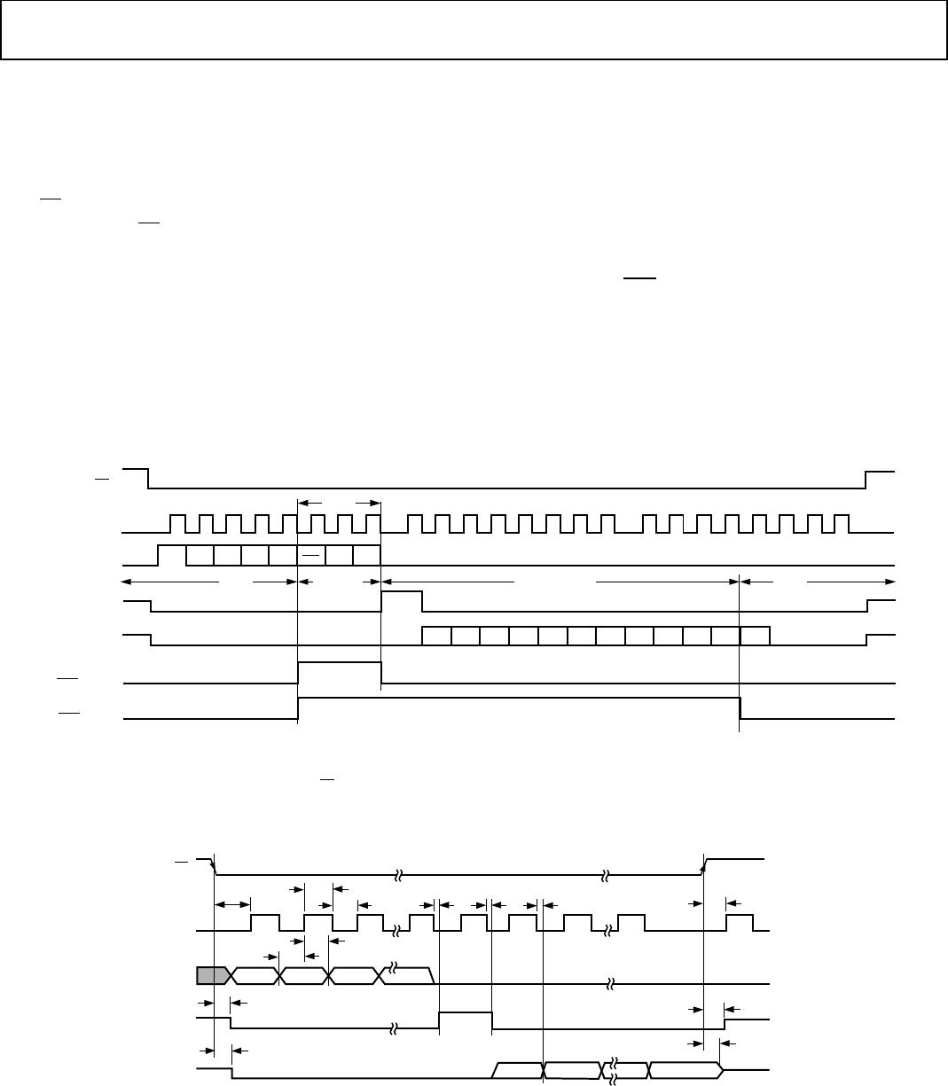
16 Clocks per Cycle
The control bits for the next conversion can be overlapped with
the current conversion to allow for a conversion every 16 DCLK
cycles, as shown in Figure 38. This timing diagram also allows
the possibility of communication with other serial peripherals
between each byte (eight DCLKs) transfer between the
processor and the converter. However, the conversion must
complete within a short enough time frame to avoid capacitive
droop effects that could distort the conversion result. It should
also be noted that the AD7873 is fully powered while other
serial communications are taking place between byte transfers.
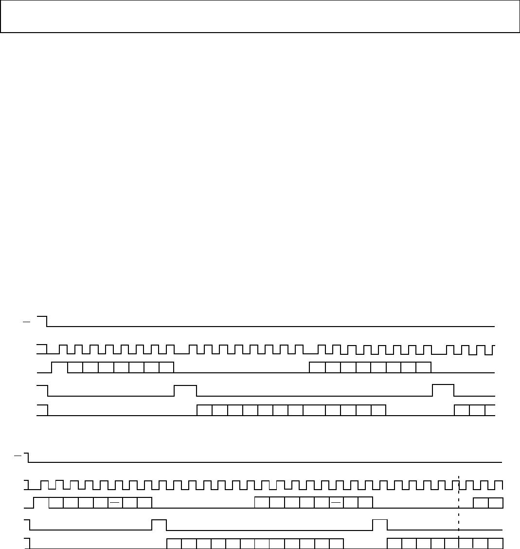
15 Clocks per Cycle
Figure 39 shows the fastest way to clock the AD7873. This
scheme does not work with most microcontrollers or DSPs
because they are not capable of generating a 15 clock cycle per
serial transfer. However, some DSPs allow the number of clocks
per cycle to be programmed. This method can also be used with
FPGAs (field programmable gate arrays) or ASICs (application
specific integrated circuits). As in the 16 clocks per cycle case,
the control bits for the next conversion are overlapped with the
current conversion to allow a conversion every 15 DCLK cycles
using 12 DCLKs to perform the conversion and 3 DCLKs to
acquire the analog input. This effectively increases the
throughput rate of the AD7873 beyond that used for the
specifications that are tested using 16 DCLKs per cycle, and
DCLK = 2 MHz.
8-Bit Conversion
The AD7873 can be set up to operate in an 8-bit mode rather
than a 12-bit mode by setting the MODE bit in the control
register to 1. This mode allows a faster throughput rate to be
achieved, assuming 8-bit resolution is sufficient. When using 8-bit
mode, a conversion is complete four clock cycles earlier than in
12-bit mode. This can be used with serial interfaces that provide
12 clock transfers, or two conversions can be completed with
three 8-clock transfers. The throughput rate increases by 25% as
a result of the shorter conversion cycle, but the conversion itself
can occur at a faster clock rate because the internal settling time
of the AD7873 is not as critical, because settling to eight bits is
all that is required. The clock rate can be as much as 50% faster.
The faster clock rate and fewer clock cycles combine to provide
double the conversion rate.
Figure 38. Conversion Timing, 16 DCLKs per Cycle, 8-Bit Bus Interface. No DCLK delay required with dedicated serial port.
Figure 39. Conversion Timing, 15 DCLKs per Cycle, Maximum Throughput Rate
DCLK
DIN
BUSY
DOUT
CS
1
S S
11 10 9 8 7 6 5 4 3 2 1 0 11 10 9
1 1
1
8 8
8
CONTROL BITS CONTROL BITS
02164-038
CS
DCLK
DIN
BUSY
DOUT
S A2 PD1 PD0A1 A0
MODE
SER/
DFR
MODE
SER/
DFR
1
11 10 9 8 7 6 5 4 3 2 1 0 11 10 9 8 7 6 5 4
15 1 15
1
S A2 S A2A1 PD1 PD0A0
02164-039
Data Sheet AD7873
Rev. F | Page 23 of 28
GROUNDING AND LAYOUT
For information on grounding and layout considerations for the
AD7873, refer to Application Note AN-577, Layout and
Grounding Recommendations for Touch Screen Digitizers.
PCB DESIGN GUIDELINES FOR
CHIP SCALE PACKAGE
The lands on the chip scale package (CP-32) are rectangular.
The printed circuit board pad for these should be 0.1 mm
longer than the package land length and 0.05 mm wider than
the package land width. The land should be centered on the
pad. This ensures that the solder joint size is maximized.
The bottom of the chip scale package has a central thermal pad.
The thermal pad on the printed circuit board should be at least
as large as this exposed pad. On the printed circuit board, there
should be a clearance of at least 0.25 mm between the thermal
pad and the inner edges of the pad pattern. This ensures that
shorting is avoided.
Thermal vias can be used on the printed circuit board thermal
pad to improve thermal performance of the package. If vias are
used, they should be incorporated in the thermal pad at 1.2 mm
pitch grid. The via diameter should be between 0.3 mm and
0.33 mm and the via barrel should be plated with 1 oz. copper
to plug the via.
The user should connect the printed circuit board thermal
pad to GND.

AD7873BRQZ-REEL

Mfr. #:
Manufacturer:
Analog Devices Inc.
Description:
Touch Screen Controllers 27V 12-BIT TouchScrn Digitizer
Lifecycle:
New from this manufacturer.
Delivery:
DHL FedEx Ups TNT EMS
Payment:
T/T Paypal Visa MoneyGram Western Union