AD7873 Data Sheet
Rev. F | Page 18 of 28
PEN INTERRUPT REQUEST
The pen interrupt equivalent circuitry is outlined in Figure 33.
By connecting a pull-up resistor (10 kΩ to 100 kΩ) between +V
CC
and this CMOS logic open-drain output, the
PENIRQ
output
remains high normally. If
PENIRQ
is enabled (see Tabl e 8), when
the touch screen connected to the AD7873 is touched by a pen
or finger, the
PENIRQ
output goes low, initiating an interrupt to
a microprocessor. This can then instruct a control word to be
written to the AD7873 to initiate a conversion. This output can
also be enabled between conversions during power-down (see
Table 8), allowing power-up to be initiated only when the
screen is touched. The result of the first touch screen coordinate
conversion after power-up is valid, assuming any external
reference is settled to the 12-bit or 8-bit level as required.
Figure 34 assumes that the
PENIRQ
function was enabled in
the last write or that the part was just powered up so
PENIRQ
is
enabled by default. Once the screen is touched, the
PENIRQ
output goes low a time t
PEN
later. This delay is approximately
5 µs, assuming a 10 nF touch screen capacitance, and varies
with the touch screen resistance actually used. Once the START
bit is detected, the pen interrupt function is disabled and
the
PENIRQ
cannot respond to screen touches. The
PENIRQ
output remains low until the fourth falling edge of DCLK after
the START bit is clocked in, at which point it returns high as
soon as possible, irrespective of the touch screen capacitance.
This does not mean that the pen interrupt function is now
enabled again because the power-down bits have not yet been
loaded to the control register. Regardless of whether
PENIRQ
is
to be enabled again, the
PENIRQ
output normally always idles
high. Assuming the
PENIRQ
is enabled again as shown in
Figure 34, then once the conversion is complete, the
PENIRQ
output again responds to a screen touch. The fact that
PENIRQ
returns high almost immediately after the fourth falling edge of
DCLK means the user avoids any spurious interrupts on the
microprocessor or DSP, which can occur if the interrupt request
line on the micro/DSP were unmasked during or toward the
end of conversion and the
PENIRQ
pin was still low. Once the
next start bit is detected by the AD7843, the
PENIRQ
function
is again disabled.
If the control register write operation overlaps with the data
read, a start bit is always detected prior to the end of
conversion, meaning that even if the
PENIRQ
function is
enabled in the control register, it is disabled by the start bit
again before the end of the conversion is reached, so
the
PENIRQ
function effectively cannot be used in this mode.
However, as conversions are occurring continuously,
the
PENIRQ
function is not necessary and is therefore
redundant.
Figure 33.
PENIRQ
Functional Block Diagram
Figure 34.
PENIRQ
Timing Diagram
Y+
Y–
ON
X+
TOUCH
SCREEN
EXTERNAL
PULL-UP
PENIRQ
ENABLE
+V
CC
+V
CC
PENIRQ
100k
02164-033
S A2 A1 A0 1 0
81 1 13 16
MODE
SER/
DFR
SCREEN
TOUCHED
HERE
NO RESPONSE TO TOUCH
t
PEN
PENIRQ
CS
DCLK
DIN
(START)
PD1 = 1, PD0 = 0, PENIRQ
ENABLED AGAIN
INTERRUPT
P
ROCESSOR
02164-034
Data Sheet AD7873
Rev. F | Page 19 of 28
CONTROL REGISTER
The control word provided to the ADC via the DIN pin is
shown in Tabl e 7. This provides the conversion start, channel
addressing, ADC conversion resolution, configuration, and
power-down of the AD7873. Table 7 provides detailed
information on the order and description of these control bits
within the control word.
Initiate START
The first bit, the S bit, must always be set to 1 to initiate the start
of the control word. The AD7873 ignores any inputs on the
DIN line until the start bit is detected.
Channel Addressing
The next three bits in the control register, A2, A1, and A0, select
the active input channel(s) of the input multiplexer (see Table 6
and Figure 26), touch screen drivers, and the reference inputs.
Mode
The MODE bit sets the resolution of the analog-to-digital
converter. With a 0 in this bit, the following conversion has
12 bits of resolution. With a 1 in this bit, the following
conversion has eight bits of resolution.
SER/
DFR
The SER/
DFR
bit controls the reference mode, set to either
single-ended or differential when a 1 or a 0 is written to this bit,
respectively. The differential mode is also referred to as the
ratiometric conversion mode. This mode is optimum for
X-position, Y-position, and pressure-touch measurements. The
reference is derived from the voltage at the switch drivers,
which is almost the same as the voltage to the touch screen. In
this case, a separate reference voltage is not needed because the
reference voltage to the ADC is the voltage across the touch
screen. In single-ended mode, the reference voltage to the
converter is always the difference between the V
REF
and GND
pins. See Table 6 and Figure 26 through Figure 29 for further
information.
If X-position, Y-position, and pressure touch are measured in
single-ended mode, an external reference voltage or +V
CC
is
required for maximum dynamic range. The internal reference
can be used for these single-ended measurements; however, a
loss in dynamic range is incurred. If an external reference is
used, the AD7873 should also be powered from the external
reference. Because the supply current required by the device is
so low, a precision reference can be used as the supply source to
the AD7873. It might also be necessary to power the touch
screen from the reference, which can require 5 mA to 10 mA. A
REF19x voltage reference can source up to 30 mA, and, as such,
could supply both the ADC and the touch screen. Care must be
taken, however, to ensure that the input voltage applied to the
ADC does not exceed the reference voltage and therefore the
supply voltage. See the Absolute Maximum Ratings section.
Note that the differential mode can only be used for X-position,
Y-position, and pressure touch measurements. All other
measurements require single-ended mode.
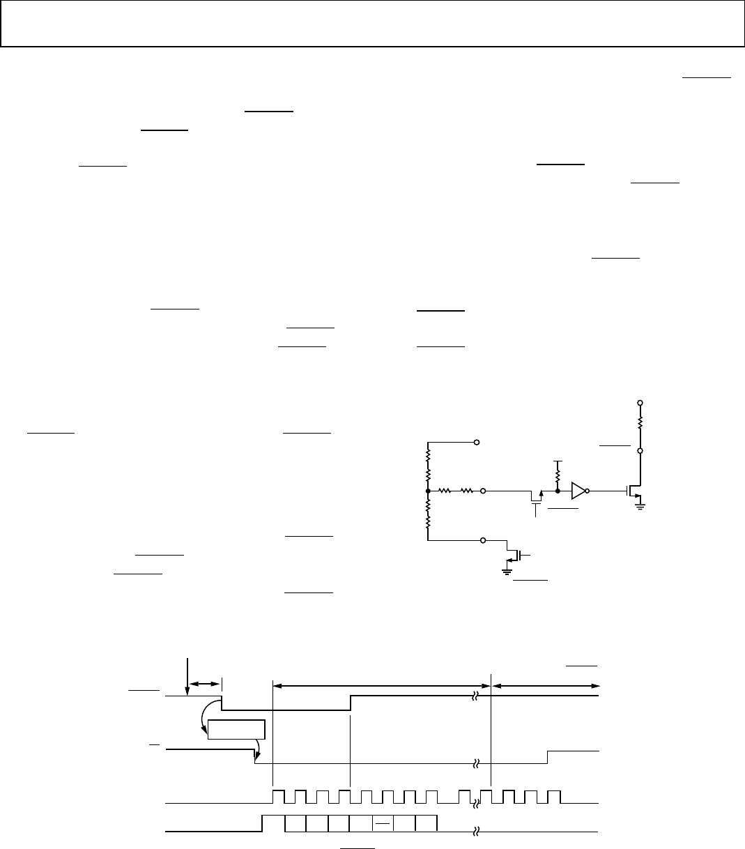
PD0 and PD1
The power management options are selected by programming
the power management bits, PD0 and PD1, in the control
register. Table 8 summarizes the options available and the
internal reference voltage configurations. The internal reference
can be turned on or off independent of the analog-to-digital
converter, allowing power saving between conversions using the
power management options. On power-up, PD0 defaults to 0,
while PD1 defaults to 1.
MSB
LSB
S A2 A1 A0 MODE SER/DFR PD1 PD0
Table 7. Control Register Bit Function Description
Bit No. Mnemonic Comment
7 S
Start Bit. The control word starts with the first high bit on DIN. A new control word can start every 15th DCLK cycle
when in the 12-bit conversion mode or every 11th DCLK cycle when in 8-bit conversion mode.
6 to 4 A2 to A0
Channel Select Bits. These three address bits along with the SER/DFR bit control the setting of the multiplexer
input, switches, and reference inputs, as detailed in Table 6.
3 MODE
12-Bit/8-Bit Conversion Select Bit. This bit controls the resolution of the following conversion. With a 0 in this bit,
the conversion has 12-bit resolution or, with a 1 in this bit, 8-bit resolution.
2
SER/
DFR Single-Ended/Differential Reference Select Bit. Together with Bit A2 to Bit A0, this bit controls the setting of the
multiplexer input, switches, and reference inputs as described in Table 6.
1, 0
PD1, PD0
Power Management Bits. These two bits decode the power-down mode of the AD7873 as shown in Table 8.
AD7873 Data Sheet
Rev. F | Page 20 of 28
Table 8. Power Management Options
PD1 PD0
PENIRQ
Description
0 0 Enabled
This configuration results in immediate power-down of the on-chip reference as soon as PD1 is set to 0. The ADC
powers down only between conversions. When PD0 is set to 0, the conversion is performed first and the ADC
powers down upon completion of that conversion (or upon the rising edge of
CS, if it occurs first). At the start of
the next conversion, the ADC instantly powers up to full power. This means if the device is being used in the
differential mode, or an external reference is used, there is no need for additional delays to ensure full operation
and the very first conversion is valid. The Yswitch is on while in power-down. When the device is performing
differential table conversions, the reference and reference buffer do not attempt to power up with Bit PD1 and
Bit PD0 programmed in this way.
0 1 Enabled
This configuration results in switching the reference off immediately and the ADC on permanently. When the
device is performing differential tablet conversions, the reference and reference buffer do not attempt to power
up with Bit PD1 and Bit PD0 programmed in this way.
1 0 Enabled
This configuration results in switching the reference on and powering the ADC down between conversions. The
ADC powers down only between conversions. When PD0 is set to 0, the conversion is performed first, and the
ADC powers down upon completion of the conversion (or upon the rising edge of CS if it occurs first). At the start
of the next conversion, the ADC instantly powers up to full power. There is no need for additional delays to ensure
full operation as the reference remains permanently powered up.
1 1 Disabled This configuration results in always keeping the device powered up. The reference and the ADC are on.
POWER VS. THROUGHPUT RATE
By using the power-down options on the AD7873 when not
converting, the average power consumption of the device
decreases at lower throughput rates. Figure 35 shows how, as
the throughput rate is reduced while maintaining the DCLK
frequency at 2 MHz, the device remains in its power-down state
longer and the average current consumption over time drops
accordingly.
Figure 35. Supply Current vs. Throughput (µA)
For example, if the AD7873 is operated in a 24-DCLK continuous
sampling mode, with a throughput rate of 10 kSPS and a DCLK
of 2 MHz, and the device is placed in the power-down mode
between conversions, (PD0, PD1 = 0, 0), that is, the ADC shuts
down between conversions but the reference remains powered
down permanently, then the current consumption is calculated
as follows. The current consumption during normal operation
with a 2 MHz DCLK is 210 µA (V
CC
= 2.7 V). Assuming an
external reference is used, the power-up time of the ADC is
instantaneous, so when the part is converting, it consumes
210 µA. In this mode of operation, the part powers up on the
fourth falling edge of DCLK after the start bit is recognized. It
goes back into power-down at the end of conversion on the
20th falling edge of DCLK, meaning that the part consumes
210 µA for 16 DCLK cycles only, 8 µs during each conversion
cycle. If the throughput rate is 10 kSPS, the cycle time is 100 µs
and the average power dissipated during each cycle is
(8/100) × (210 µA) = 16.8 µA.
SUPPLY CURRENT (µA)
1
100
10
1000
0 120
THROUGHPUT (kSPS)
40 600 20 80 100
f
DCLK
= 16 × f
SAMPLE
f
DCLK
= 2MHz
V
CC
= 2.7V
T
A
= –40°C TO +85°C
02164-035

AD7873BRQZ-REEL

Mfr. #:
Manufacturer:
Analog Devices Inc.
Description:
Touch Screen Controllers 27V 12-BIT TouchScrn Digitizer
Lifecycle:
New from this manufacturer.
Delivery:
DHL FedEx Ups TNT EMS
Payment:
T/T Paypal Visa MoneyGram Western Union