Jitter Attenuator & FemtoClock
®
Multiplier
ICS813252I-02
DATA SHEET
ICS813252CKI-02 REVISION A AUGUST 4, 2016 1 ©2016 Integrated Device Technology, Inc.
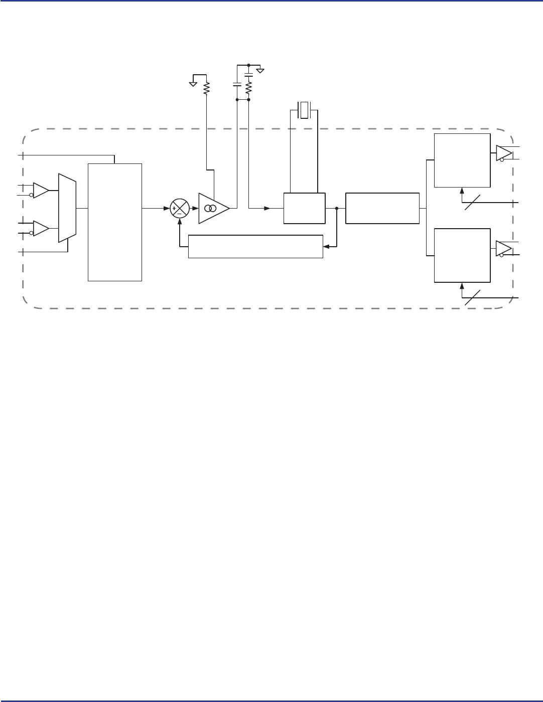
GENERAL DESCRIPTION
The ICS813252I-02 is a PLL based synchronous multiplier that is
optimized for PDH or SONET to Ethernet clock jitter attenuation
and frequency translation. The device contains two internal
frequency multiplication stages that are cascaded in series. The fi rst
stage is a VCXO PLL that is optimized to provide reference clock
jitter attenuation. The second stage is a FemtoClock
®
frequency
multiplier that provides the low jitter, high frequency Ethernet
output clock that easily meets Gigabit and 10 Gigabit Ethernet jitter
requirements. Pre-divider and output divider multiplication ratios
are selected using device selection control pins. The multiplication
ratios are optimized to support most common clock rates used in
PDH, SONET and Ethernet applications. The VCXO requires the
use of an external, inexpensive pullable crystal. The VCXO uses
external passive loop fi lter components which allows confi guration
of the PLL loop bandwidth and damping characteristics. The
device is packaged in a space-saving 32-VFQFN package and
supports industrial temperature range.
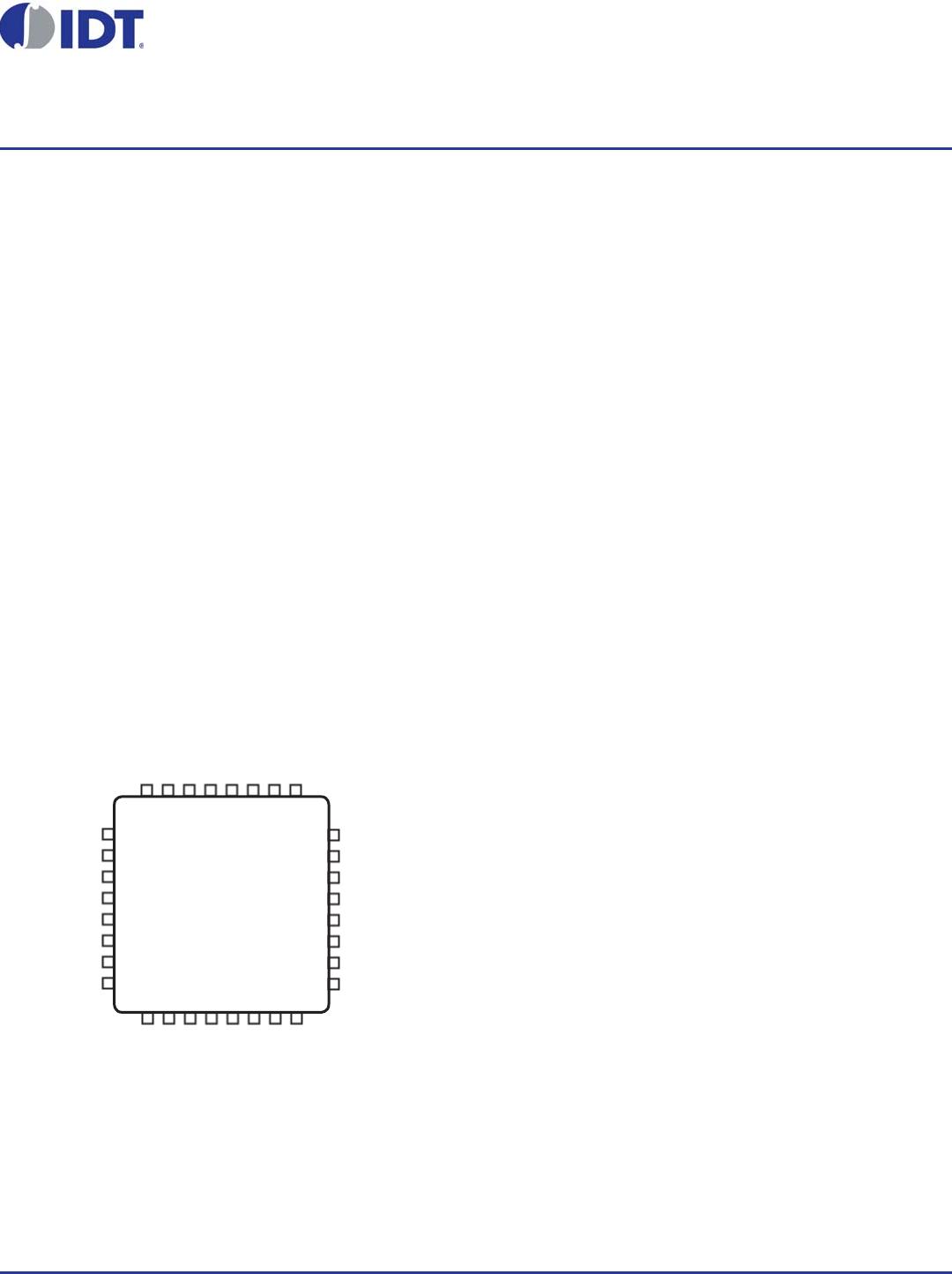
PIN ASSIGNMENT
FEATURES
• Two LVPECL outputs
Each output supports independent frequency selection at
25MHz, 125MHz, 156.25MHz and 312.5MHz
• Two differential inputs support the following input types: LVPE-
CL, LVDS, LVHSTL, SSTL, HCSL
• Accepts input frequencies from 8kHz to 155.52MHz including
8kHz, 1.544MHz, 2.048MHz, 19.44MHz, 25MHz, 77.76MHz,
125MHz and 155.52MHz
• Attenuates the phase jitter of the input clock by using a low-
cost pullable fundamental mode VCXO crystal
• VCXO PLL bandwidth can be optimized for jitter attenuation
and reference tracking
using external loop fi lter connection
• FemtoClock frequency multiplier provides low jitter, high fre-
quency output
• Absolute pull range: 50ppm
• FemtoClock VCO frequency: 625MHz
•
RMS phase jitter @ 125MHz, using a 25MHz crystal
(10kHz – 20MHz): 1.3ps (maximum)
• 3.3V supply voltage
•
-40°C to 85°C ambient operating temperature
• Available in lead-free (RoHS 6) package
• For functional replacement device use 813N252CKI-02LF
32 31 30 29 28 27 26 25
9 10 11 12 13 14 15 16
1
2
3
4
5
6
7
8
24
23
22
21
20
19
18
17
V
EE
nQB
QB
VCCO
nQA
QA
VEE
ODASEL_0
ICS813252I-02
PDSEL_2
PDSEL_1
PDSEL_0
VCC
VCCA
ODBSEL_1
ODBSEL_0
ODASEL_1
nCLK1
CLK1
VCC
nCLK0
CLK0
XTAL_OUT
XTAL_IN
VCCX
LF1
LF0
ISET
VEE
CLK_SEL
VCC
RESERVED
VEE
32-Lead VFQFN
5mm x 5mm x 0.925 package body
K Package
Top View
OBSOLETE