ICS813252CKI-02 REVISION A AUGUST 4, 2016 12 ©2016 Integrated Device Technology, Inc.
ICS813252I-02 Data Sheet VCXO JITTER ATTENUATOR & FEMTOCLOCK
®
MULTIPLIER
INPUTS:
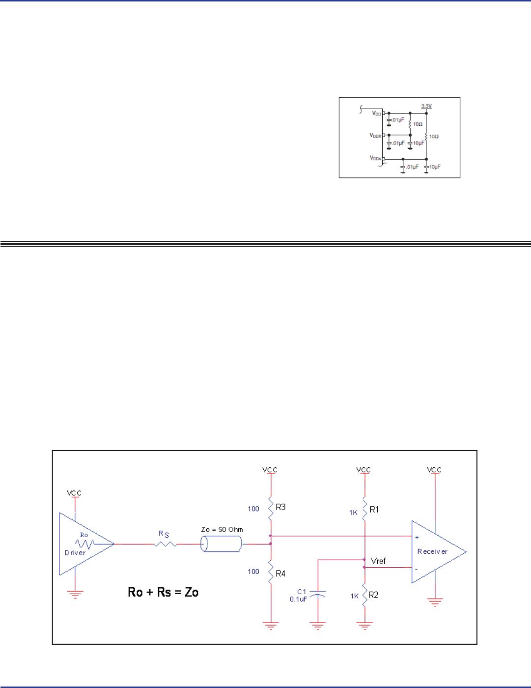
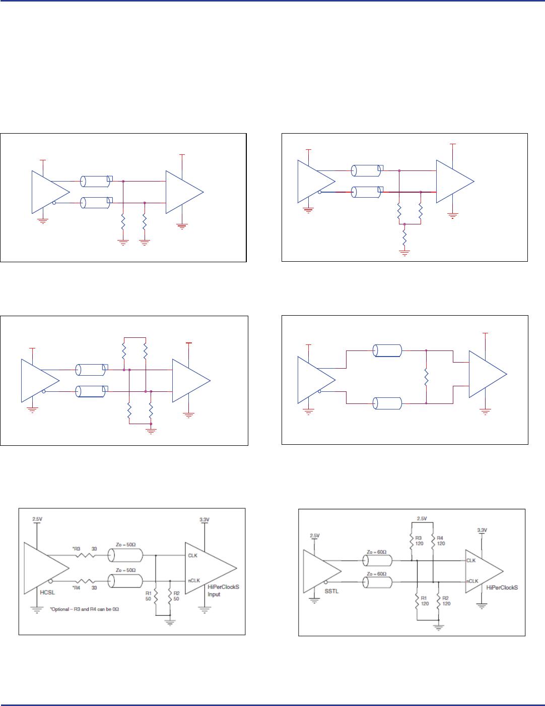
CLK/nCLK INPUTS
For applications not requiring the use of the differential input, both
CLK and nCLK can be left fl oating. Though not required, but for
additional protection, a 1kΩ resistor can be tied from CLK to ground.
LVCMOS C
ONTROL PINS
All control pins have internal pull-ups or pull-downs; additional
resistance is not required but can be added for additional protection.
A 1kΩ resistor can be used.
OUTPUTS:
LVPECL OUTPUTS
RECOMMENDATIONS FOR UNUSED INPUT AND OUTPUT PINS
All unused LVPECL outputs can be left fl oating. We recommend
that there is no trace attached. Both sides of the differential output
pair should either be left fl oating or terminated.
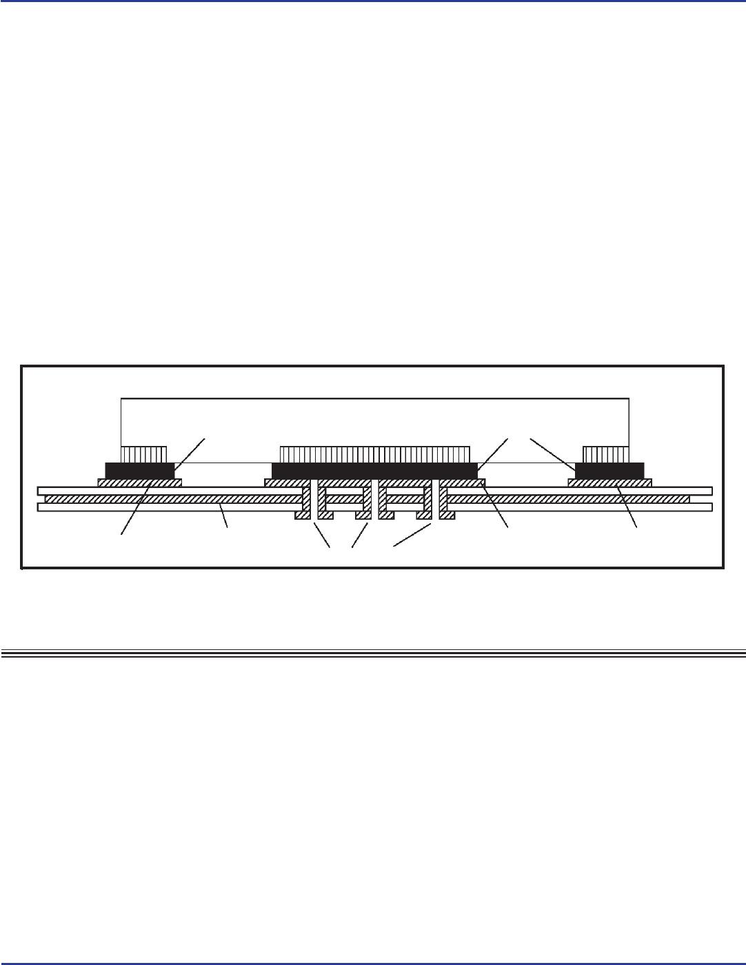
FIGURE 4. P.C.ASSEMBLY FOR EXPOSED PAD THERMAL RELEASE PATH –SIDE VIEW (DRAWING NOT TO SCALE)
VFQFN EPAD THERMAL RELEASE PATH
In order to maximize both the removal of heat from the package and
the electrical performance, a land pattern must be incorporated on
the Printed Circuit Board (PCB) within the footprint of the package
corresponding to the exposed metal pad or exposed heat slug on
the package, as shown in Figure 4. The solderable area on the PCB,
as defi ned by the solder mask, should be at least the same size/
shape as the exposed pad/slug area on the package to maximize
the thermal/electrical performance. Suffi cient clearance should be
designed on the PCB between the outer edges of the land pattern
and the inner edges of pad pattern for the leads to avoid any shorts.
While the land pattern on the PCB provides a means of heat transfer
and electrical grounding from the package to the board through a
solder joint, thermal vias are necessary to effectively conduct from
the surface of the PCB to the ground plane(s). The land pattern
must be connected to ground through these vias. The vias act as
“heat pipes”. The number of vias (i.e. “heat pipes”) are application
specifi c and dependent upon the package power dissipation as well
as electrical conductivity requirements. Thus, thermal and electrical
analysis and/or testing are recommended to determine the minimum
number needed. Maximum thermal and electrical performance is
achieved when an array of vias is incorporated in the land pattern.
It is recommended to use as many vias connected to ground as
possible. It is also recommended that the via diameter should be 12
to 13mils (0.30 to 0.33mm) with 1oz copper via barrel plating. This
is desirable to avoid any solder wicking inside the via during the
soldering process which may result in voids in solder between the
exposed pad/slug and the thermal land. Precautions should be taken
to eliminate any solder voids between the exposed heat slug and
the land pattern. Note: These recommendations are to be used as a
guideline only. For further information, refer to the Application Note
on the Surface Mount Assembly of Amkor’s Thermally/Electrically
Enhance Leadfame Base Package, Amkor Technology.
SOLDERSOLDER
PINPIN EXPOSED HEAT SLUG
PIN PAD PIN PADGROUND PLANE LAND PATTERN
(GROUND PAD)
THERMAL VIA