ICS813252CKI-02 REVISION A AUGUST 4, 2016 19 ©2016 Integrated Device Technology, Inc.
ICS813252I-02 Data Sheet VCXO JITTER ATTENUATOR & FEMTOCLOCK
®
MULTIPLIER
PACKAGE OUTLINE AND DIMENSIONS - K SUFFIX FOR 32 LEAD VFQFN
To p View
Index Area
D
Cham fer 4x
0.6 x 0.6 max
OPTIONAL
Anvil
Singula tion
A
0. 08 C
C
A3
A1
S eating Plan e
E2
E2
2
L
(N
-1)x e
(R ef.)
(Ref.)
N & N
Even
N
e
D2
2
D2
(Ref.)
N & N
Odd
1
2
e
2
(Ty p.)
If N & N
are Even
(N -1)x e
(Re f.)
b
Th er mal
Base
N
OR
Anvil
Singulation
N-1N
CHAMFER
1
2
N-1
1
2
N
RADIUS
N-1
1
2
N
AA
DD
CC
BB
4
4
4
4
4
4
Bottom View w/Type B ID Bottom View w/Type C IDBottom View w/Type A ID
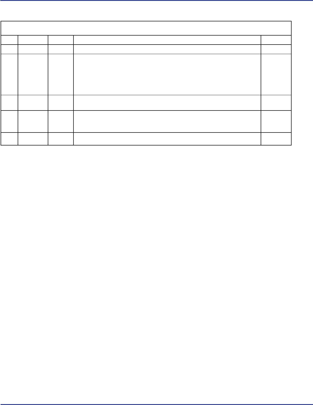
There are 3 methods of indicating pin 1 corner
at the back of the VFQFN package are:
1. Type A: Chamfer on the paddle (near pin 1)
2. Type B: Dummy pad between pin 1 and N.
3. Type C: Mouse bite on the paddle (near pin 1)
JEDEC VARIATION
ALL DIMENSIONS IN MILLIMETERS (VHHD -2/ -4)
SYMBOL Minimum Maximum
N
32
A
0.80 1.0
A1
0 0.05
A3
0.25 Reference
b
0.18 0.30
e
0.50 BASIC
N
D
8
N
E
8
D, E
5.0 BASIC
D2, E2
3.0 3.3
L
0.30 0.50
NOTE: The above mechanical package drawing is a generic drawing
that applies to any pin count VFQFN package. This drawing is not
intended to convey the actual pin count or pin layout of this device.
The pin count and pinout are shown on the front page. The package
dimensions are in Table 8.
Reference Document: JEDEC Publication 95, MO-220
TABLE 8. PACKAGE DIMENSIONS