ICS813252CKI-02 REVISION A AUGUST 4, 2016 15 ©2016 Integrated Device Technology, Inc.
ICS813252I-02 Data Sheet VCXO JITTER ATTENUATOR & FEMTOCLOCK
®
MULTIPLIER
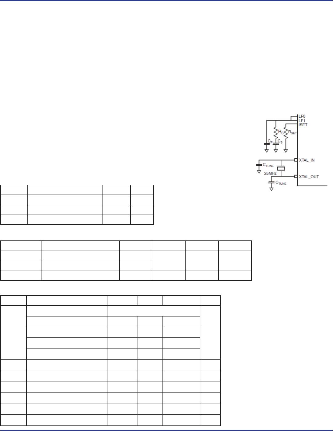
VCXO-PLL EXTERNAL COMPONENTS
Choosing the correct external components and having a proper
printed circuit board (PCB) layout is a key task for quality operation
of the VCXO-PLL. In choosing a crystal, special precaution
must be taken with the package and load capacitance (C
L
). In
addition, frequency, accuracy and temperature range must also be
considered. Since the pulling range of a crystal also varies with the
package, it is recommended that a metal-canned package like HC49
be used. Generally, a metal-canned package has a larger pulling
range than a surface mounted device (SMD). For crystal selection
information, refer to the VCXO Crystal Selection Application Note.
The crystal’s load capacitance C
L
characteristic determines its
resonating frequency and is closely related to the VCXO tuning
range. The total external capacitance seen by the crystal when
installed on a board is the sum of the stray board capacitance, IC
package lead capacitance, internal varactor capacitance and any
installed tuning capacitors (C
TUNE
).
If the crystal’s C
L
is greater than the total external capacitance,
the VCXO will oscillate at a higher frequency than the crystal
specifi cation. If the crystal’s C
L
is lower than the total external
capacitance, the VCXO will oscillate at a lower frequency than the
VCXO-PLL APPROXIMATE LOOP BANDWIDTH SELECTION TABLE
Bandwidth Crystal Frequency (MHz)
R
S
(kΩ)
C
S
(µF) C
P
(µF)
R
SET
(kΩ)
10Hz (Low) 25MHz 121 1.0 0.01 9.09
90Hz (Mid) 25MHz 221 0.1 0.001 2.21
300Hz (High) 25MHz 680 0.1 0.0001 2.21
CRYSTAL CHARACTERISTICS
VCXO CHARACTERISTICS TABLE
Symbol Parameter
Minimum Typical Maximum Units
Mode of Operation Fundamental
f
N
Frequency 25 MHz
f
T
Frequency Tolerance ±20 ppm
f
S
Frequency Stability ±20 ppm
Operating Temperature Range -40 85 °C
C
L
Load Capacitance 10 pF
C
O
Shunt Capacitance 4 pF
C
O
/C
1
Pullability Ratio 220 240
ESR Equivalent Series Resistance 20
Drive Level 1 mW
Aging @ 25°C ±3 per year ppm
Symbol Parameter
Typical Unit
k
VCXO
VCXO Gain 15,700 Hz/V
C
V_LOW
Low Varactor Capacitance 9.9 pF
C
V_HIGH
High Varactor Capacitance 22.2 pF
crystal specifi cation. In either case, the absolute tuning range is
reduced. The correct value of C
L
is dependent on the characteristics
of the VCXO. The recommended C
L
in the Crystal Parameter Table
balances the tuning range by centering the tuning curve.
The VCXO-PLL Loop Bandwidth Selection Table shows R
S
, C
S
and C
P
values for recommended high, mid and low loop bandwidth
confi gurations. The device has been characterized using these
parameters. For other configurations, refer to the Loop Filter
Component Selection for VCXO Based PLLs Application Note.
The crystal and external loop fi lter components should be kept as
close as possible to the device. Loop fi lter and crystal traces should
be kept short and separated from
each other. Other signal traces
should be kept separate and not
run underneath the device, loop
fi lter or crystal components.

