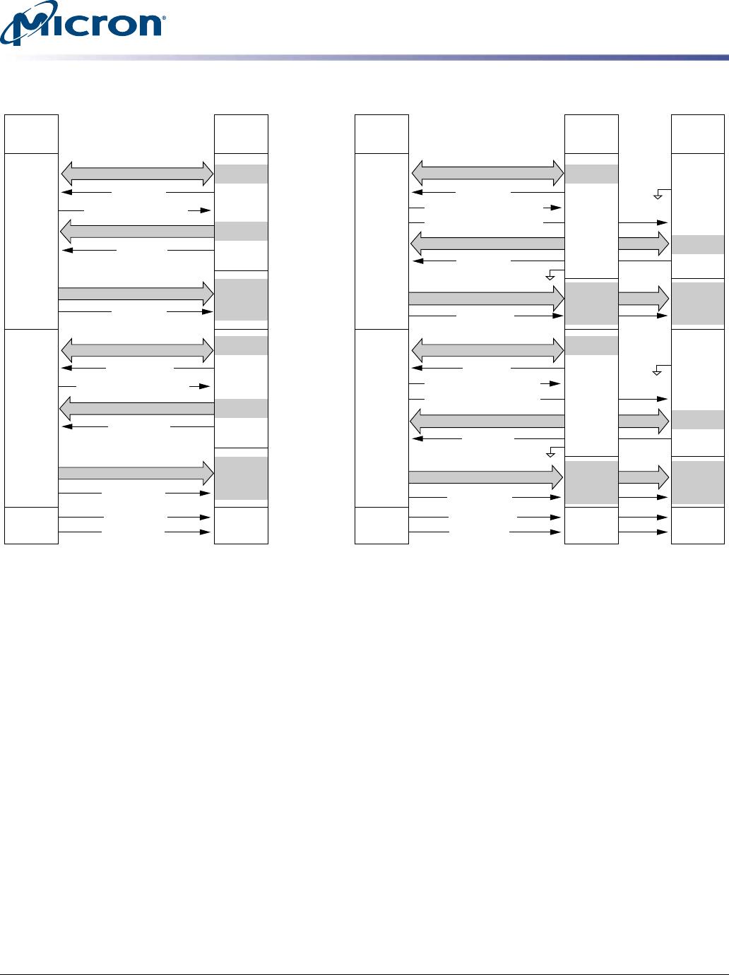
Figure 10: Byte Orientation in Clamshell Topology
x8
x8
Legend:
Data
ADD/CMD
CK, WCK
x8 top
x8 bottom
Ch A
Byte
0
Ch B
Byte
1
Ch A
Byte
0
Ch B
Byte
1
Ch A
Byte
0
Ch B
Byte
1
Ch A
Byte
1
Ch B
Byte
0
+ =
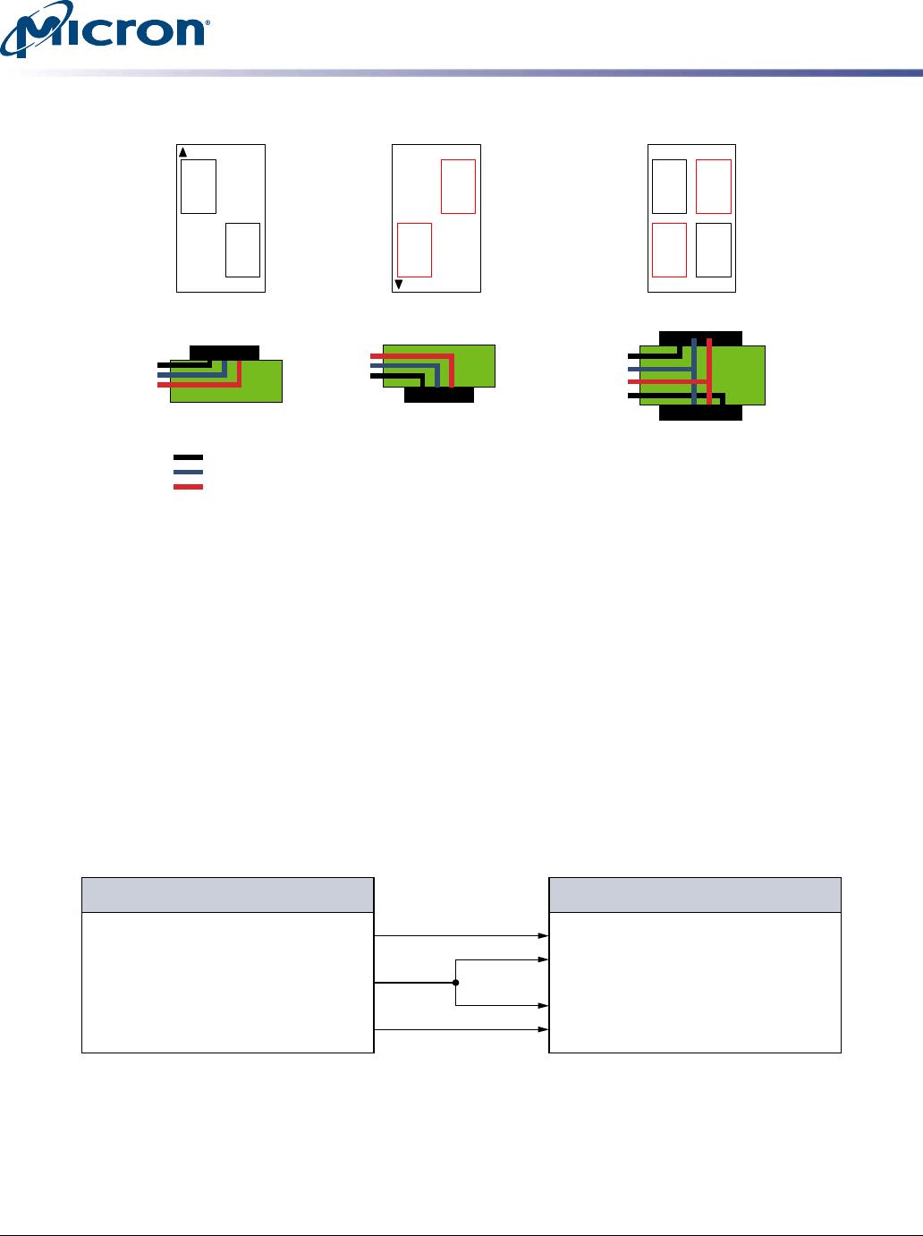
Pseudo-Channel Mode
GDDR6 has been optimized for a 32B access across a 16-bit channel by providing a
unique CA bus to each 16-bit-wide channel. For applications requiring fewer CA pins,
GDDR6 includes support for a pseudo-channel (PC) mode where CA[9:4], CKE_n, and
CABI_n on each channel are connected to a common bus, while CA[3:0] of each chan-
nel are connected to a separate bus. The command truth table is organized such that in
PC mode the same command is decoded in both pseudo-channels, but READ and
WRITE commands support a unique column address to each pseudo-channel. In PC
mode, CKE_n and CABI_n are also shared across pseudo-channels.
In PC mode, the only difference in the DRAM is that termination on CA[9:4], CKE_n,
and CABI_n can be configured differently from CA[3:0]. PC mode can be selected during
initialization by driving CA6 = LOW on both channels when RESET_n is driven HIGH.
Figure 11: CA Pins in Pseudo-Channel Mode
GDDR6
CA[3:0]_A
CA[9:4]_A, CABI_n_A, CKE_n_A
CA[9:4]_B, CABI_n_B, CKE_n_B
CA[3:0]_B
CA[3:0]_A
CA[9:4], CABI_n, CKE_n
CA[3:0]_B
Pseudo-Channel Mode Controller
8Gb: 2 Channels x16/x8 GDDR6 SGRAM
Functional Description
CCMTD-1412786195-10191
gddr6_sgram_8gb_brief.pdf - Rev. F 8/18 EN
14
Micron Technology, Inc. reserves the right to change products or specifications without notice.
© 2016 Micron Technology, Inc. All rights reserved.