© Freescale Semiconductor, Inc., 2006 - 2008. All rights reserved.
Freescale Semiconductor
Technical Data
This document contains information on a product under development. Freescale reserves the right to change or discontinue this
product without notice.
Document Number: MC13853
Rev. 1.8, 8/2008
MC13853
Package Information
Plastic Package
(QFN–16)
Ordering Information
Device
Device Marking or
Operating
Temperature Range
Package
MC13853 853 QFN-16
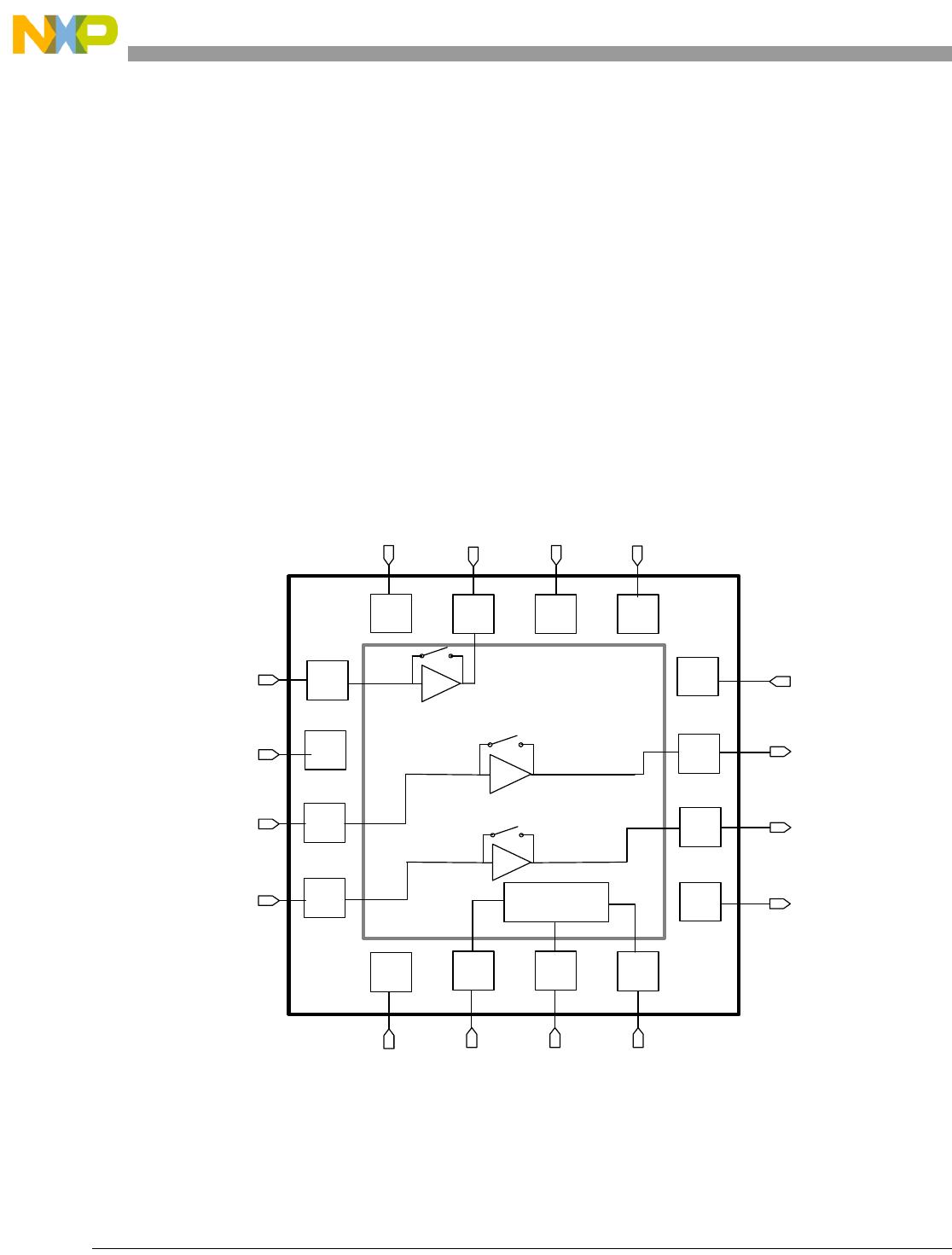
1 Introduction
The MC13853 is a SPI controlled, tri-band, high gain
LNA with extremely low noise figure, designed for
cellular band applications. Integrated bypass switches
are included to preserve input intercept performance.
The input and output match are external to allow
maximum design flexibility. The MC13853 is fabricated
using Freescale's advanced RF BiCMOS process using
the SiGe:C option and is packaged in the QFN-16
leadless package.
1.1 Features
• RF input frequency: 800 MHz to 2.4 GHz
• Gain: 13.5 dB (typical) at 1960 MHz, 15 dB
(typical) at 2140 MHz, and 13.5 dB (typical) at
880 MHz
• Input 3rd order intercept point (IIP3): -3 dBm
(typical) at 880 MHz, -4.0 dBm (typical) at 1960
MHz, and -3.0 dBm (typical) at 2140 MHz
• Noise figure (NF): 1.5 dB (typical) at 880 MHz,
1.5 dB (typical) at 1960 MHz, and 1.6 dB
(typical) at 2140 MHz
MC13853
Tri-Band Low Noise Amplifiers
with Bypass Switches
Contents
1 Introduction . . . . . . . . . . . . . . . . . . . . . . . . . . 1
2 Electrical Specifications . . . . . . . . . . . . . . . . 3
3 Application Information . . . . . . . . . . . . . . . . . 9
4 Packaging . . . . . . . . . . . . . . . . . . . . . . . . . . . 23
5 Product Documentation . . . . . . . . . . . . . . . . 25