Electrical Specifications
MC13853 Technical Data, Rev. 1.8
4 Freescale Semiconductor
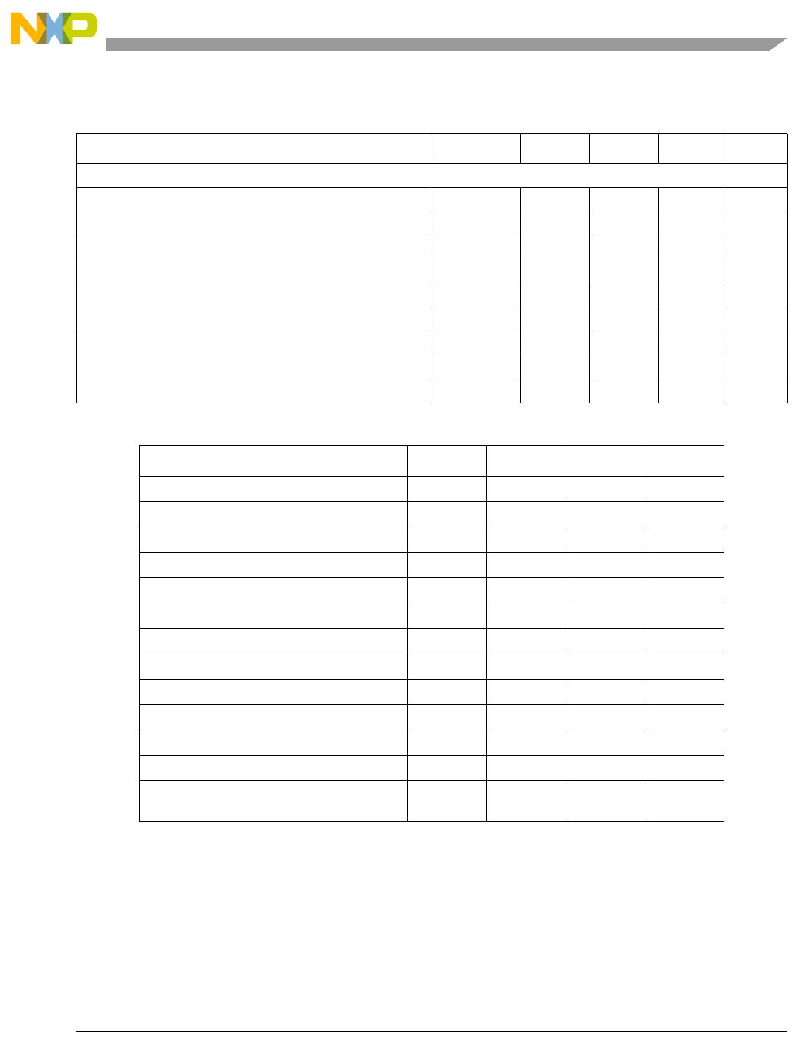
Bypass Gain G -10 -9.5 dB
Bypass Input Third Order Intercept Point IIP3 16 22 dBm
Bypass Current 10 20 µA
950 MHz (Refer to Figure 5)
Frequency f 925 950 960 MHz
Active Gain G 11.0 12.0 13.0 dB
Active Noise Figure NF 1.45 1.5 dB
Active Input Third Order Intercept Point IIP3 -3 -2.5 dBm
Active Input 1 dB Compression Point P
1dB
-9 -8.5 dBm
Active Current @ 2.75 V in current setting 6 I
CC
8.6 10.2 mA
Bypass Gain G -10 -9.5 dB
Bypass Input Third Order Intercept Point IIP3 16 22 dBm
Bypass Current 10 20 µA
1850 MHz (Refer to Figure 6)
Frequency f 1805 1850 1880 MHz
Active Gain G 12.5 13.5 14.5 dB
Active Noise Figure NF 1.55 1.6 dB
Active Input Third Order Intercept Point IIP3 -3 -2.5 dBm
Active Input 1 dB Compression Point P
1dB
-12.5 -11.7 dBm
Active Current @ 2.75 V in current setting 6 I
CC
–7.89.7mA
Bypass Gain G -9.5 -9 dB
Bypass Input Third Order Intercept Point IIP3 16 22 dBm
Bypass Current 10 20 µA
1960 MHz (Refer to Figure 7)
Frequency f 1930 1960 1990 MHz
Active Gain G 12.5 13.5 14.5 dB
Active Noise Figure NF 1.55 1.6 dB
Active Input Third Order Intercept Point IIP3 -3 -2.5 dBm
Active Input 1 dB Compression Point P
1dB
-12.5 -12 dBm
Active Current @ 2.75 V in current setting 6 I
CC
–7.89.7mA
Bypass Gain G -9.5 -9 dB
Bypass Input Third Order Intercept Point IIP3 20 22 dBm
Bypass Current 10 20 µA
Table 3. Electrical Characteristics in Frequency Specific Tuned Circuits (continued)
(V
CC
= 2.775 V, 25°C)
Characteristic Symbol Minimum Typical Maximum Unit
Electrical Specifications
MC13853 Technical Data, Rev. 1.8
Freescale Semiconductor 5
2140 MHz (Refer to Figure 8)
Frequency f 2110 2140 2170 MHz
Active Gain G 14 15 16 dB
Active Noise Figure NF 1.55 1.6 dB
Active Input Third Order Intercept Point IIP3 -3 -2.5 dBm
Active Input 1 dB Compression Point P
1dB
-12 -11 dBm
Active Current @ 2.75 V in current setting 2 I
CC
–6.07.0mA
Bypass Gain G -6.5 -6 dB
Bypass Input Third Order Intercept Point IIP3 20 22 dBm
Bypass Current 10 20 µA
Table 4. Electrical Characteristics Over Temperature (-30°C to 85°C)
Characteristic Symbol Minimum Maximum Unit
High Gain Mode Current Icc mA
LNA1 HB2 8.3
LNA2 HB1 11.5
LNA3 LB 10.2
Bypass Mode Current Icc 30 µA
Active Gain Variation Across Temperature G dB
85°C relative to 25°C -1.0 +0.5
-30°C relative to 25°C -0.5 +1.0
GdB
85°C relative to 25°C -1.0 +0.5
-30°C relative to 25°C -0.5 +1.0
Noise Figure relative to 25°CNF +0.4dB
Active Input Third Order Intercept relative to
25°C
IIP3 -2.0 dBm
Table 3. Electrical Characteristics in Frequency Specific Tuned Circuits (continued)
(V
CC
= 2.775 V, 25°C)
Characteristic Symbol Minimum Typical Maximum Unit
Electrical Specifications
MC13853 Technical Data, Rev. 1.8
6 Freescale Semiconductor
Table 5. Truth Table for SPI Operation
Mode Gain Bit Enable Bit
Active 1 1
Bypass Gain 0 0
Disable 1 0
Not Used 0 1
Note: At power on reset (POR), the mode is set to
bypass gain on all LNAs.
Table 6. SPI Programmable Current Draw (25°C)
SPI bit Typical Current (mA)
Current
Setting
Current 2 Current 1 Current 0 LNA 1 HB2 LNA 2 HB1 LNA3 LB
0007.48.08.6 0
0014.44.55.0 1
010
5.3 5.6 6.2 2
0 1 1 9.1 9.8 10.8 3
1001.82.22.0 4
1016.26.57.2 5
1107.17.7 8.3 6
1 1 1 9.8 11.0 11.9 7
Default current setting shown in gray for each band
Table 7. Maximum Current
25
°C-30°C to 85°C Unit
Deep Sleep Mode - Vcc on and VDDauxSPI off 1 5 µ
A
VDDauxSPI during a read operation 400 400 µA

MC13853FCR2

Mfr. #:
Manufacturer:
NXP / Freescale
Description:
RF Amplifier IOTA TRI-BAND LNA P2.1
Lifecycle:
New from this manufacturer.
Delivery:
DHL FedEx Ups TNT EMS
Payment:
T/T Paypal Visa MoneyGram Western Union

Products related to this Datasheet