Application Information
MC13853 Technical Data, Rev. 1.8
Freescale Semiconductor 11
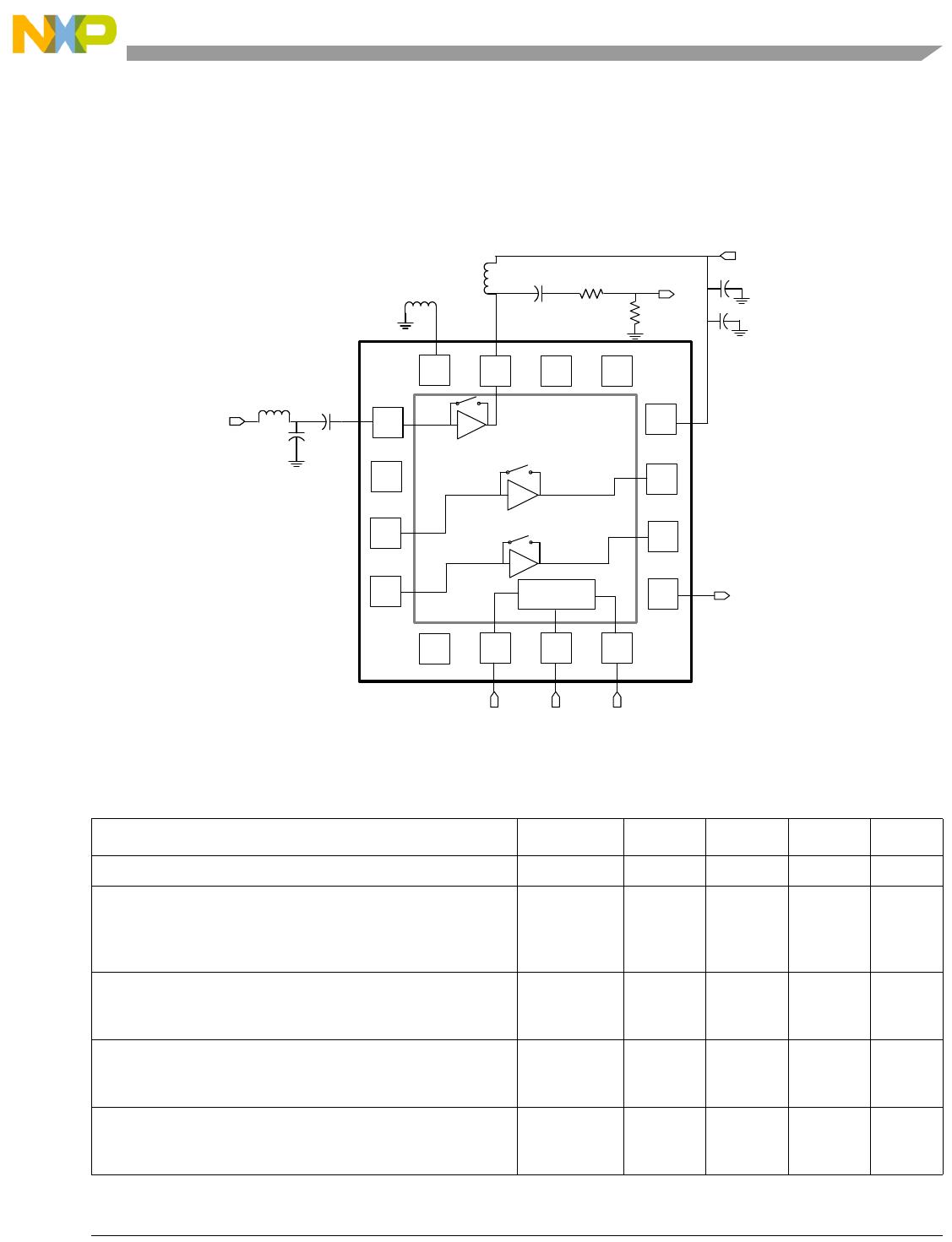
3.1 880 MHz Application
This application circuit was designed to provide NF 1.5 dB, typical S21 gain of 13.5 dB, IIP3 of -3 dBm.
Typical performance that can be expected from this circuit at 2.775 V V
CC
is listed in Table 9. The
component values can be changed to enhance the performance of a particular parameter, but usually at the
expense of another.
Figure 4. 880 MHz LNA Application Schematic
Table 9. Typical 880 MHz LNA Demo Board Performance (
25°C)
Characteristic Symbol Min Typ Max Unit
Frequency f 869 880 894 MHz
Power Gain
High Gain Band V
High Gain Band VI
Bypass
G
12.5
12.5
-10
13.5
13.5
-9.5
14.5
14.5
–
dB
Input Third Order Intercept Point
High Gain
Bypass
IIP3
-3
16
-2.5
22
–
–
dBm
In Ref P1dB
High Gain
Bypass
P
1dBin
-9.5
0
-9
3.5
–
–
dBm
Noise Figure
High Gain
Bypass
NF
–
–
1.45
3
1.5
6
dB
1
2
6 7
8
15 14 13
11
12
10
SPI Clk
SPI FrmSPI Data
LB
LNA IN
LB LNA
OUT
3
9
Vcc
4
5
16
VDDauxSPI
SPI
Triband
LNA Die
L1
10 nH
C1
5.6 pf
C10
10 pf
L5
18 nH
R4
62
C11
33 pf
C12
.01uf
QFN16
16 pin
3x3x0.85 mm
Package
LB Emit
Remit
O ohm
Rs
82
C1
0.5 pf