Application Information
MC13853 Technical Data, Rev. 1.8
Freescale Semiconductor 17
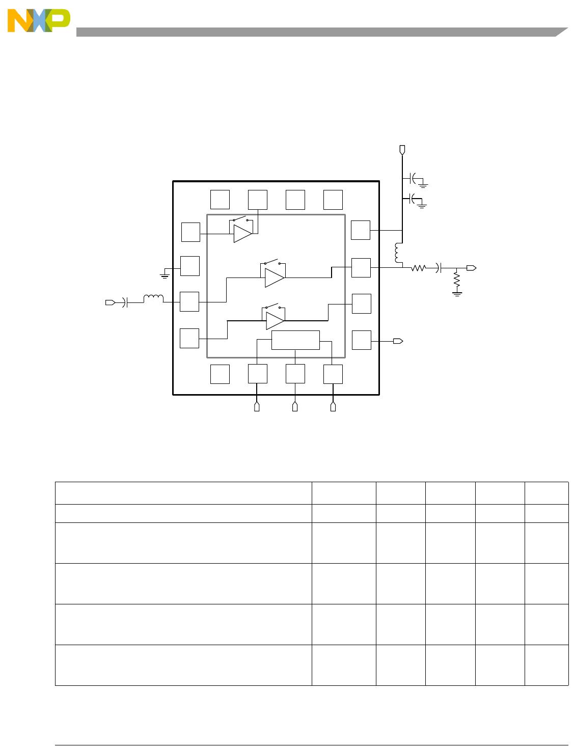
3.4 1960 MHz Application
This application circuit is designed to demonstrate performance at 1960 MHz. Typical performance that
can be expected from this circuit at 2.775 V V
CC
is listed in Table 12. The match consists of a highpass
match on the output and a simple inductor-capacitor network on the LNA input.
Figure 7. 1960 MHz LNA Application Schematic
Table 12. Typical 1960 MHz LNA Demo Board Performance (
25°C)
Characteristic Symbol Min Typ Max Unit
Frequency f 1930 1850 1990 MHz
Power Gain
High Gain
Bypass
G
12.5
-9.5
13.5
-9
14.5
–
dB
Input Third Order Intercept Point
High Gain
Bypass
IIP3
-3
16
-2.5
22
–
–
dBm
In Ref P1dB
High Gain
Bypass
P
1dBin
-12.5
0
-12
3.5
–
–
dBm
Noise Figure
High Gain
Bypass
NF
–
–
1.6
3
1.7
6
dB
1
2
6 7
8
15 14 13
11
12
10
SPI Clk
HB1
LNA IN
SPI Frm
SPI Data
3
9
Vcc
HB1 LNA
OUT
4
5
16
VDDauxSPI
SPI
Triband
LNA Die
HB1 Emit
L2
3.9 nH
C2
10 pF
C5
33 pf
C6
.01uf
R2
75
C8
10 pf
L6
4.7 nH
R5
30
QFN16
16 pin
3 x 3 x 0.85 mm
Package