Electrical Specifications
MC13853 Technical Data, Rev. 1.8
Freescale Semiconductor 7
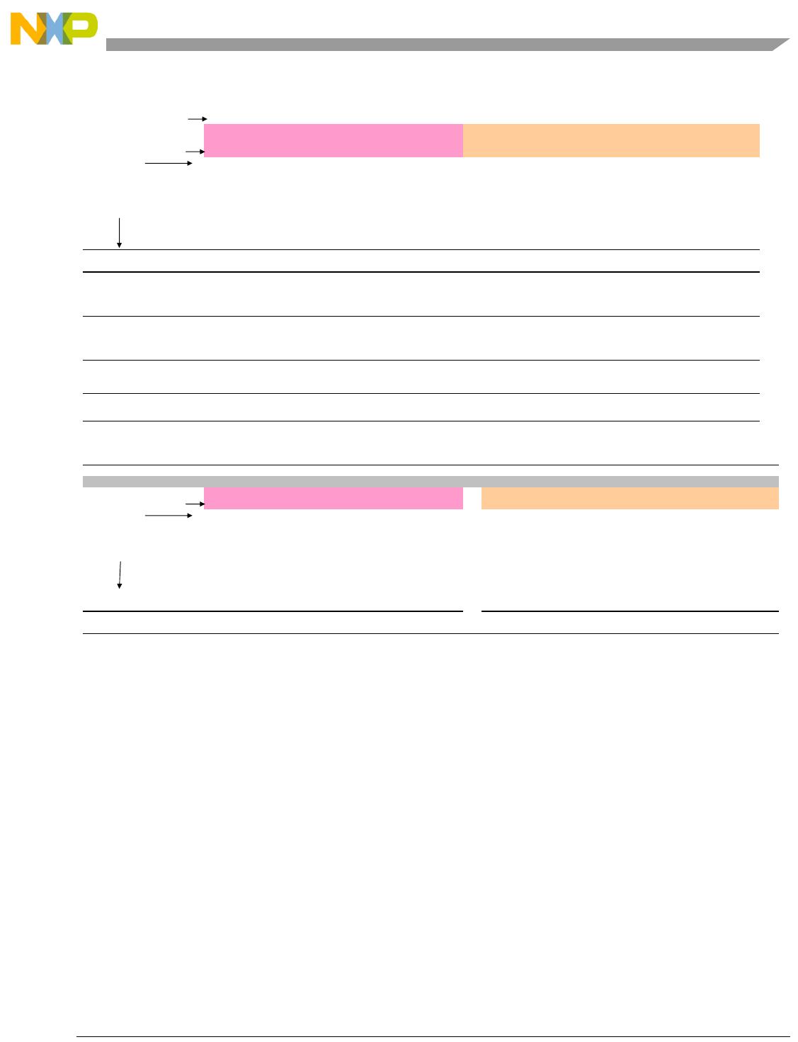
Figure 2. SPI Bit Word
SPI bit word
Cloc
k
123456789101112131415161718192021222324252627282930
Address structur
e
Data Structure
Bit # 29 28 27 26 25 24 23 22 21 20 19 18 17 16 15 14 13 12 11 10 9876543210
Not Variable 1010000100
Variable
Write / Read Bit
Device Type is LNA
Device Type is LNA
Device Type is LNA
Device is Iota
Device is Iota
Device is Iota
Device is Iota
Device is Iota
LNA Selector PA4
LNA Selector PA3
LNA Selector PA2
LNA Selector PA1
LNA Selector PA0
Current 2
Current 1
Current 0
Enable
Gain
SPI Data Write
0
Read
1
LNA Selecto
LNA1 HB2 000
LNA2 HB1 001
LNA3 LB 010
GPO (Ext LNA) 100
Mode Selecto
r
Active 11
Bypass 00
Disable 01
Not Used 10
Current Selecto
r
LNA1 HB2 010
(default) LNA2 HB1 110
LNA3 LB 110
GPO2
GPO1
Mode Selecto
r
Active 11
for GPO Bypass 10
(External LNA) Disable 00
Disable 01
Read Mod
e
Address structur
e
Data Structure
Bit # 29 28 27 26 25 24 23 22 21 20 19 18 17 16 15 14 13 12 11 10 9876543210
Not Variable 1010000100
Variable
HID
8
HID
7
HID
6
HID
5
HID
4
HID
3
HID
2
HID
1
HID
0
SPI Data Read
1
LNA Selecto
For Hardware Read 011
one extra clock cycle in read mode
Electrical Specifications
MC13853 Technical Data, Rev. 1.8
8 Freescale Semiconductor
Table 8. SPI Used for Dual-, Tri-, and Quad-Band Configurations
SPI Inputs
LNA Selector Enable Gain Outputs
PATH #
Bit
22
Bit
21
PA2 PA1 PA0 D2 D1 G P O1 GPO2 Mo de
Dual- or
Tri-band
Config
Tri-band
LNA #1
1 0 1 0 0 0 1 1 No Connect No Connect LNA1 Active LNAs 1,
2, and 3
or LNAs
1 and 2
1 0 1 0 0 0 0 0 No Connect No Connect LNA1 Bypass
1 0 1 0 0 0 0 1 No Connect No Connect LNA1 Off
2 0 1 0 0 1 1 1 No Connect No Connect LNA2 Active
2 0 1 0 0 1 0 0 No Connect No Connect LNA2 Bypass
2 0 1 0 0 1 0 1 No Connect No Connect LNA2 Off
3 0 1 0 1 0 1 1 No Connect No Connect LNA3 Active
3 0 1 0 1 0 0 0 No Connect No Connect LNA3 Bypass
3 0 1 0 1 0 0 1 No Connect No Connect LNA 3 Off
Note: This is an SPI-controlled, tri-band MC13853 LNA.
Quad-
band
Config
Tri-band
LNA #1
1 0 1 0 0 0 1 1 To Ext LNA To Ext LNA LNA1 Active LNAs 1,
2, 3, and
4
1 0 1 0 0 0 0 0 To Ext LNA To Ext LNA LNA1 Bypass
1 0 1 0 0 0 0 1 To Ext LNA To Ext LNA LNA1 Off
2 0 1 0 0 1 1 1 To Ext LNA To Ext LNA LNA2 Active
2 0 1 0 0 1 0 0 To Ext LNA To Ext LNA LNA2 Bypass
2 0 1 0 0 1 0 1 To Ext LNA To Ext LNA LNA2 Off
3 0 1 0 1 0 1 1 To Ext LNA To Ext LNA LNA3 Active
3 0 1 0 1 0 0 0 To Ext LNA To Ext LNA LNA3 Bypass
3 0 1 0 1 0 0 1 To Ext LNA To Ext LNA LNA3 Off
Single
LNA
4 0 1 1 0 0 1 1 NA NA LNA4 Active
401100 10 NA NA LNA4 Bypass
401100 00 NA NA LNA4 Off
Note: This is one SPI-controlled, tri-band MC13853 LNA and one external LNA (not a MC13853) controlled by GPO from the
MC13853 LNA.
The different banding LNA combinations are:
Dual band (using one MC13853)
Tri-band (using one MC13853)
Quad-band (using one MC13853 and one single-band GPO-controlled external LNA (not a MC13853))
Application Information
MC13853 Technical Data, Rev. 1.8
Freescale Semiconductor 9
3 Application Information
The MC13853 SiGe:C LNA is designed for applications in the 800 MHz to 2.1 GHz range. It has three
different modes: High Gain, Low Gain (Bypass) and Disabled. The IC mode is programmable through the
Gain and Enable bits. The current setting is also SPI programmable. The logic truth table is given in
Table 5.
In these application examples a balance is made between the competing RF performance characteristics of
I
CC
, NF, gain, IP3 and return losses with unconditional stability. Conjugate matching is not used for the
input or output. Instead, matching which achieves a trade-off in RF performance qualities is utilized. For
a particular application or spec requirement, the matching can be changed to achieve enhanced
performance of one parameter at the expense of other parameters.
Application information for 880, 950, 1800, 1960, and 2140 MHz are shown. Measurements are made at
a bias of V
CC
= 2.775 V. Freq. spacing for IP3 measurements is 800 kHz for 2G and 10 MHz for 3GPP.
The board loss corrections for these boards are: Input 0.16 dB, Output 0.2 dB. NF results incorporate these
corrections in order to better reflect the actual performance of the device.
Two MC13853 devices can also be used with common SPI control lines for a quad-band application, as
shown in Figure 3. In this application, LB and HB1 are used on LNA1 and HB2 is used on LNA2. In
active mode, both LNAs are active, but only one is connected in the circuit. Depending on which band is
selected in the connected LNA, the corresponding un-connected LNA which would also become active
when the SPI command is sent to the connected LNA will draw <1 mA for LB, <1.2 mA for HB1 and
<1mA for HB2 in active mode over temperature.

MC13853FCR2

Mfr. #:
Manufacturer:
NXP / Freescale
Description:
RF Amplifier IOTA TRI-BAND LNA P2.1
Lifecycle:
New from this manufacturer.
Delivery:
DHL FedEx Ups TNT EMS
Payment:
T/T Paypal Visa MoneyGram Western Union

Products related to this Datasheet