Application Information
MC13853 Technical Data, Rev. 1.8
Freescale Semiconductor 13
3.2 950 MHz Application
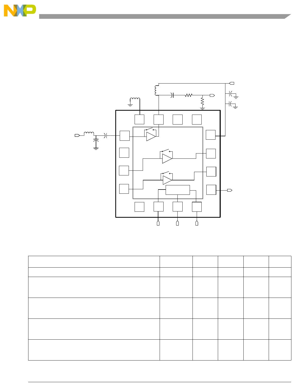
This application circuit was designed to provide NF < 1.5 dB, S21 gain of 12 dB, IIP3 of -3 dBm. Typical
performance that can be expected from this circuit at 2.775 V V
CC
is listed in Table 10. The component
values can be changed to enhance the performance of a particular parameter, but usually at the expense of
another.
Figure 5. 950 MHz LNA Application Schematic
Table 10. Typical 950 MHz LNA Demo Board Performance (
25°C)
Characteristic Symbol Min Typ Max Unit
Frequency f 925 950 960 MHz
Power Gain
High Gain
Bypass
G
11
-10
12
-9.5
13
dB
Input Third Order Intercept Point
High Gain
Bypass
IIP3
-3
16
-2.5
22
dBm
In Ref P1dB
High Gain
Bypass
P
1dBin
-9
0
-8.5
3.5
dBm
Noise Figure
High Gain
Bypass
NF
1.45
3
1.5
6
dB
1
2
6 7
8
15 14 13
11
12
10
SPI Clk
SPI FrmSPI Data
LB
LNA IN
LB LNA
OUT
3
9
Vcc
4
5
16
VDDauxSPI
SPI
Triband
LNA Die
L1
10 nH
C1
5.6 pf
C10
10 pf
L5
18 nH
R4
62
C11
33 pf
C12
.01uf
QFN16
16 pin
3x3x0.85 mm
Package
LB Emit
Remit
O ohm
Rs
82
C1
0.5 pf
Application Information
MC13853 Technical Data, Rev. 1.8
14 Freescale Semiconductor
Current Drain in current setting6
High Gain
Bypass
I
CC
8.5
10
10.2
20
mA
µA
Input Return Loss
High Gain
Bypass
S11
-10
-3
-11
-3.5
dB
Gain
High Gain
Bypass
S21
11
-10
12
-9.5
13
dB
Reverse Isolation
High Gain
Bypass
S12
-20
-22
-4
dB
Output Return Loss
High Gain
Bypass
S22
-10
-3
-11
-3.5
dB
P
IN
IM2
F
INT
= RX/2 at -40 dBm
IM2
-56 -57
dBm
P
IN
IM2
F
INT1
= TX at -27 dBm
F
INT2
= TX +RX at -49 dBm
-62
-63
dBm
P
IN
IM2
F
INT1
= TX at -27 dBm
F
INT2
= RX -TX at -54 dBm
-55
-56
dBm
Switching Time
From 20% top 90% of VIH
From 20% top 90% of VIL
TRISE
TFALL
5
5
µs
Table 10. Typical 950 MHz LNA Demo Board Performance (25°C) (continued)
Characteristic Symbol Min Typ Max Unit
Application Information
MC13853 Technical Data, Rev. 1.8
Freescale Semiconductor 15
3.3 1850 MHz Application
This application circuit is designed to demonstrate performance at 1850 MHz. Typical performance that
can be expected from this circuit at 2.775 V V
CC
is listed in Table 11. The match consists of a highpass
match on the output and a simple inductor-capacitor network on the LNA input.
Figure 6. 1850 MHz LNA Application Schematic
Table 11. Typical 1850 MHz LNA Demo Board Performance (
25°C)
Characteristic Symbol Min Typ Max Unit
Frequency f 1805 1850 1880 MHz
Power Gain
High Gain
Bypass
G
12.5
-9.5
13.5
-9
14.5
dB
Input Third Order Intercept Point
High Gain
Bypass
IIP3
-3
16
-2.5
22
dBm
In Ref P1dB
High Gain
Bypass
P
1dBin
-12.5
0
-11.7
3.5
dBm
Noise Figure
High Gain
Bypass
NF
1.55
3
1.6
6
dB
1
2
6 7
8
15 14 13
11
12
10
SPI Clk
HB1
LNA IN
SPI Frm
SPI Data
3
9
Vcc
HB1 LNA
OUT
4
5
16
VDDauxSPI
SPI
Triband
LNA Die
HB1 Emit
L2
3.9 nH
C2
10 pF
C5
33 pf
C6
.01uf
R2
75
C8
10 pf
L6
4.7 nH
QFN16
16 pin
3x3x0.85 mm
Package
R5
30

MC13853FCR2

Mfr. #:
Manufacturer:
NXP / Freescale
Description:
RF Amplifier IOTA TRI-BAND LNA P2.1
Lifecycle:
New from this manufacturer.
Delivery:
DHL FedEx Ups TNT EMS
Payment:
T/T Paypal Visa MoneyGram Western Union

Products related to this Datasheet