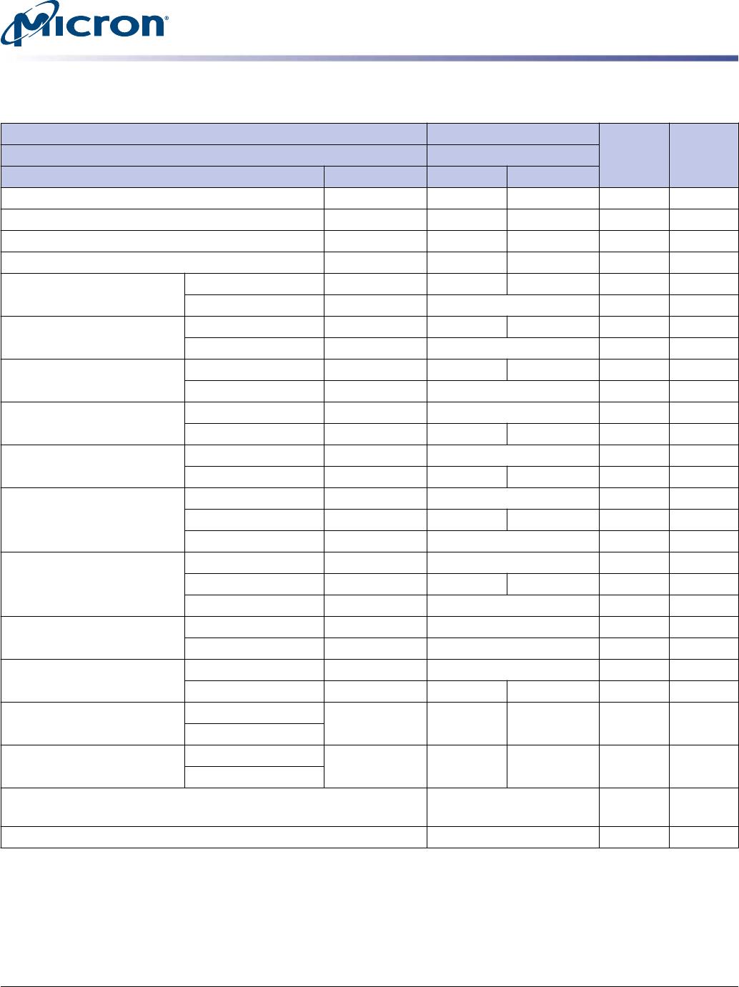
Table 11: Electrical Characteristics and AC Operating Conditions for Speed Extensions (Continued)
Notes 1–8 apply to the entire table
Parameter Symbol
gDDR3-2000 gDDR3-2200
Unit NotesMin Max Min Max
Data setup time to DQS,
DQS#
Base (specification)
t
DS
(AC150)
– – 10 – ps 18, 19
V
REF
@ 1 V/ns – – 160 – ps 19, 20
Data setup time to DQS,
DQS#
Base (specification)@
2 V/ns
t
DS
(AC135)
68 – – – ps 19, 20
V
REF
@ 2 V/ns 135 – – – 19, 20
Data hold time from
DQS, DQS#
Base (specification)
t
DH
(DC100)
70 – 70 – ps 18, 19
V
REF
@ 1 V/ns 120 – 120 – ps 19, 20
Minimum data pulse width
t
DIPW 320 – 320 – ps 41
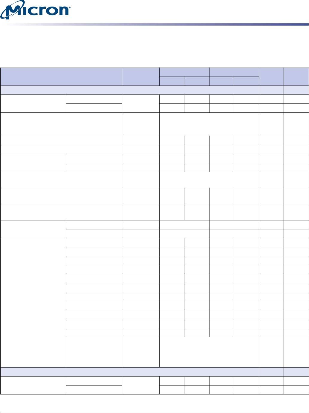
DQ Output Timing
DQS, DQS# to DQ skew, per access
t
DQSQ – 85 – 85 ps
DQ output hold time from DQS, DQS#
t
QH 0.38 – 0.38 –
t
CK
(AVG)
21
DQ Low-Z time from CK, CK#
t
LZ (DQ) –390 195 –390 195 ps 22, 23
DQ High-Z time from CK, CK#
t
HZ (DQ) – 195 – 195 ps 22, 23
DQ Strobe Input Timing
DQS, DQS# rising to CK, CK# rising
t
DQSS –0.27 0.27 –0.27 0.27 CK 25
DQS, DQS# differential input low pulse width
t
DQSL 0.45 0.55 0.45 0.55 CK
DQS, DQS# differential input high pulse width
t
DQSH 0.45 0.55 0.45 0.55 CK
DQS, DQS# falling setup to CK, CK# rising
t
DSS 0.18 – 0.18 – CK 25
DQS, DQS# falling hold from CK, CK# rising
t
DSH 0.18 – 0.18 – CK 25
DQS, DQS# differential WRITE preamble
t
WPRE 0.9 – 0.9 – CK
DQS, DQS# differential WRITE postamble
t
WPST 0.3 – 0.3 – CK
DQ Strobe Output Timing
DQS, DQS# rising to/from rising CK, CK#
t
DQSCK –195 195 –195 195 ps 23
DQS, DQS# rising to/from rising CK, CK# when
DLL is disabled
t
DQSCK
(DLL_DIS)
1 10 1 10 ns 26
DQS, DQS# differential output high time
t
QSH 0.40 – 0.40 – CK 21
DQS, DQS# differential output low time
t
QSL 0.40 – 0.40 – CK 21
DQS, DQS# Low-Z time (RL - 1)
t
LZ (DQS) –390 195 –391 195 ps 22, 23
DQS, DQS# High-Z time (RL + BL/2)
t
HZ (DQS) – 195 – 195 ps 22, 23
DQS, DQS# differential READ preamble
t
RPRE 0.9 Note 24 0.9 Note 24 CK 23, 24
DQS, DQS# differential READ postamble
t
RPST 0.3 Note 27 0.3 Note 27 CK 23, 27
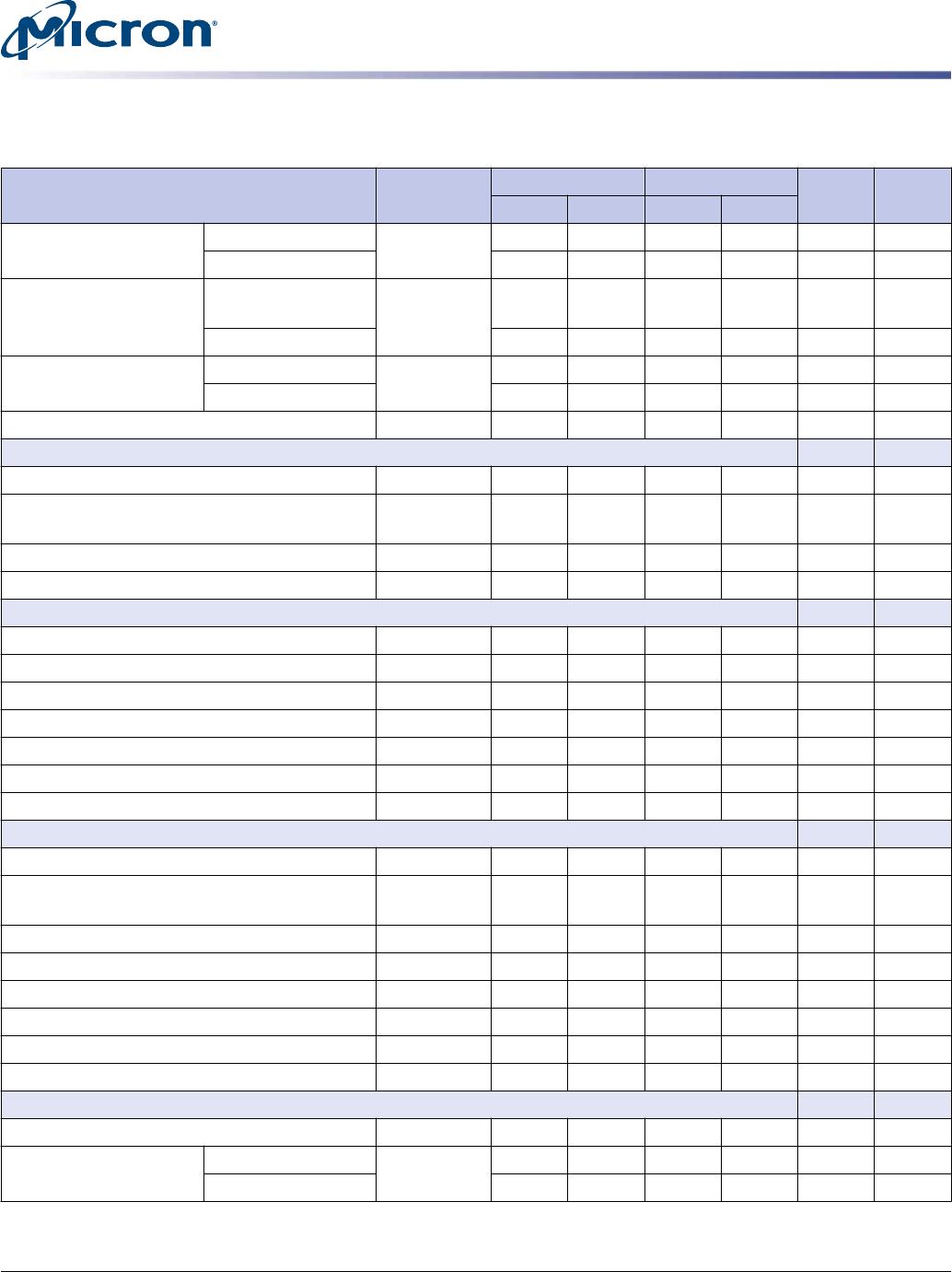
Command and Address Timing
DLL locking time
t
DLLK 512 – 512 – CK 28
CTRL, CMD, ADDR
setup to CK,CK#
Base (specification)
t
IS
(AC175)
– – 45 – ps 29, 30
V
REF
@ 1 V/ns – – 220 – ps 20, 30
4Gb: x16 gDDR3 SDRAM Graphics Addendum
Electrical Characteristics and AC Operating Conditions
CCMTD-1005363231-10344
ddr3_4gb_graphics_addendum 091.pdf - Rev. A 05/16 EN
12
Micron Technology, Inc. reserves the right to change products or specifications without notice.
© 2012 Micron Technology, Inc. All rights reserved.