Speed Bin Tables
Table 7: gDDR3-1600 Speed Bins
gDDR3-1600 Speed Bin -125G
Unit Notes
CL-
t
RCD-
t
RP 11-11-11
Parameter Symbol Min Max
ACTIVATE to internal READ or WRITE delay time
t
RCD 13.75 ns
PRECHARGE command period
t
RP 13.75 ns
ACTIVATE-to-ACTIVATE or REFRESH command period
t
RC 48.75 ns
ACTIVATE-to-PRECHARGE command period
t
RAS 35 9 x
t
REF ns 1
CL = 5 CWL = 5
t
CK (AVG) 3.0 3.3 ns 2
CWL = 6, 7, 8
t
CK (AVG) Reserved ns 3
CL = 6 CWL = 5
t
CK (AVG) 2.5 3.3 ns 2
CWL = 6, 7, 8
t
CK (AVG) Reserved ns 3
CL = 7 CWL = 5
t
CK (AVG) Reserved ns 3
CWL = 6
t
CK (AVG) 1.875 <2.5 ns 2
CWL = 7, 8
t
CK (AVG) Reserved ns 3
CL = 8 CWL = 5
t
CK (AVG) Reserved ns 3
CWL = 6
t
CK (AVG) 1.875 <2.5 ns 2
CWL = 7, 8
t
CK (AVG) Reserved ns 3
CL = 9 CWL = 5, 6
t
CK (AVG) Reserved ns 3
CWL = 7
t
CK (AVG) 1.5 <1.875 ns 2
CWL = 8
t
CK (AVG) Reserved ns 3
CL = 10 CWL = 5, 6
t
CK (AVG) Reserved ns 3
CWL = 7
t
CK (AVG) 1.5 <1.875 ns 2
CWL = 8
t
CK (AVG) Reserved ns 3
CL = 11 CWL = 5, 6, 7
t
CK (AVG) Reserved ns 3
CWL = 8
t
CK (AVG) 1.25 <1.5 ns 2
Supported CL settings 5, 6, 7, 8, 9, 10, 11 CK
Supported CWL settings 5, 6, 7, 8 CK
Notes:
1.
t
REFI depends on T
OPER
.
2. The CL and CWL settings result in
t
CK requirements. When making a selection of
t
CK,
both CL and CWL requirement settings need to be fulfilled.
3. Reserved settings are not allowed.
4Gb: x16 gDDR3 SDRAM Graphics Addendum
Speed Bin Tables
CCMTD-1005363231-10344
ddr3_4gb_graphics_addendum 091.pdf - Rev. A 05/16 EN
7
Micron Technology, Inc. reserves the right to change products or specifications without notice.
© 2012 Micron Technology, Inc. All rights reserved.
Table 8: gDDR3-1800 Speed Bins
gDDR3-1800 Speed Bin -107G
Unit Notes
CL-
t
RCD-
t
RP 13-13-13
Parameter Symbol Min Max
ACTIVATE to internal READ or WRITE delay time
t
RCD 14.3 ns
PRECHARGE command period
t
RP 14.3 ns
ACTIVATE-to-ACTIVATE or REFRESH command period
t
RC 48.91 ns
ACTIVATE-to-PRECHARGE command period
t
RAS 35 9 x
t
REFI ns 1
CL = 5 CWL = 5
t
CK (AVG) 3.0 3.3 ns 3
CWL = 6, 7, 8, 9
t
CK (AVG) Reserved ns 3
CL = 6 CWL = 5
t
CK (AVG) 2.5 3.3 ns 2
CWL = 6, 7, 8, 9
t
CK (AVG) Reserved ns 3
CL = 7 CWL = 5, 7, 8, 9
t
CK (AVG) 2.5 3.3 ns 2
CWL = 6
t
CK (AVG) Reserved ns 3
CL = 8 CWL = 5, 7, 8, 9
t
CK (AVG) Reserved ns 3
CWL = 6
t
CK (AVG) 1.875 <2.5 ns 2
CL = 9 CWL = 5, 6, 8, 9
t
CK (AVG) Reserved ns 3
CWL = 7
t
CK (AVG) 1.875 <2.5 ns 3
CL = 10 CWL = 5, 6, 9
t
CK (AVG) Reserved ns 3
CWL = 7
t
CK (AVG) 1.5 <1.875 ns 2
CWL = 8
t
CK (AVG) Reserved ns 3
CL = 11 CWL = 5, 6, 7
t
CK (AVG) Reserved ns 3
CWL = 8
t
CK (AVG) 1.5 <1.875 ns 2
CWL = 9
t
CK (AVG) Reserved ns 3
CL - 12 CWL = 5, 6, 7, 8
t
CK (AVG) Reserved ns 3
CWL = 9
t
CK (AVG) Reserved ns 3
CL = 13 CWL = 5, 6, 7, 8
t
CK (AVG) Reserved ns 3
CWL = 9
t
CK (AVG) 1.1 <1.25 ns 2
Supported CL settings 5, 6, 7, 8, 9, 10, 11, 13 CK
Supported CWL settings 5, 6, 7, 8, 9 CK
Notes:
1.
t
REFI depends on T
OPER
.
2. The CL and CWL settings result in
t
CK requirements. When making a selection of
t
CK,
both CL and CWL requirement settings need to be fulfilled.
3. Reserved settings are not allowed.
4Gb: x16 gDDR3 SDRAM Graphics Addendum
Speed Bin Tables
CCMTD-1005363231-10344
ddr3_4gb_graphics_addendum 091.pdf - Rev. A 05/16 EN
8
Micron Technology, Inc. reserves the right to change products or specifications without notice.
© 2012 Micron Technology, Inc. All rights reserved.
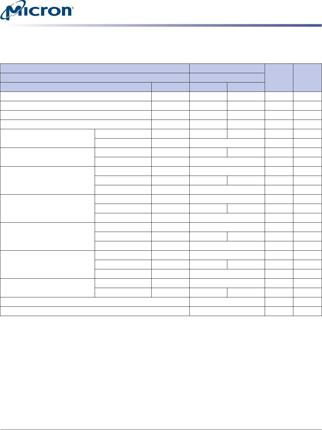
Table 9: gDDR3-2000 Speed Bins
gDDR3-2000 Speed Bin -093G
Unit Notes
CL-
t
RCD-
t
RP 14-14-14
Parameter Symbol Min Max
ACTIVATE to internal READ or WRITE delay time
t
RCD 14 ns
PRECHARGE command period
t
RP 14 ns
ACTIVATE-to-ACTIVATE or REFRESH command period
t
RC 50 ns
ACTIVATE-to-PRECHARGE command period
t
RAS 36 9 x
t
REFI ns 1
CL = 5 CWL = 5
t
CK (AVG) 3.0 3.3 ns 2
CWL = 6, 7, 8, 9
t
CK (AVG) Reserved ns 3
CL = 6 CWL = 5
t
CK (AVG) 2.5 3.3 ns 2
CWL = 6, 7, 8, 9
t
CK (AVG) Reserved ns 3
CL = 7 CWL = 5, 7, 8, 9
t
CK (AVG) 2.5 3.3 ns 3
CWL = 6
t
CK (AVG) Reserved ns 3
CL = 8 CWL = 5, 7, 8, 9
t
CK (AVG) Reserved ns 3
CWL = 6
t
CK (AVG) 1.875 <2.5 ns 2
CL = 9 CWL = 5, 6, 8, 9
t
CK (AVG) Reserved ns 3
CWL = 7
t
CK (AVG) 1.875 <2.5 ns 3
CL = 10 CWL = 5, 6, 9
t
CK (AVG) Reserved ns 3
CWL = 7
t
CK (AVG) 1.5 <1.875 ns 2
CWL = 8
t
CK (AVG) Reserved ns 3
CL = 11 CWL = 5, 6, 7
t
CK (AVG) Reserved ns 3
CWL = 8
t
CK (AVG) 1.5 <1.875 ns 3
CWL = 9
t
CK (AVG) Reserved ns 3
CL - 12 CWL = 5, 6, 7, 8
t
CK (AVG) Reserved ns 3
CWL = 9
t
CK (AVG) Reserved ns 3
CL = 13 CWL = 5, 6, 7, 8
t
CK (AVG) Reserved ns 3
CWL = 9
t
CK (AVG) 1.1 <1.25 ns 2
CL = 14 CWL = 5, 6, 7, 8, 9
t
CK (AVG) 1 <1.1 ns 2
CWL = 10
Supported CL settings 5, 6, 7, 8, 9, 10, 11, 13, 14 CK
Supported CWL settings 5, 6, 7, 8, 9, 10 CK
Notes:
1.
t
REFI depends on T
OPER
.
2. The CL and CWL settings result in
t
CK requirements. When making a selection of
t
CK,
both CL and CWL requirement settings need to be fulfilled.
3. Reserved settings are not allowed.
4Gb: x16 gDDR3 SDRAM Graphics Addendum
Speed Bin Tables
CCMTD-1005363231-10344
ddr3_4gb_graphics_addendum 091.pdf - Rev. A 05/16 EN
9
Micron Technology, Inc. reserves the right to change products or specifications without notice.
© 2012 Micron Technology, Inc. All rights reserved.

MT41J256M16LY-091G:N

Mfr. #:
Manufacturer:
Micron
Description:
IC DRAM 4G PARALLEL 1GHZ 96FBGA
Lifecycle:
New from this manufacturer.
Delivery:
DHL FedEx Ups TNT EMS
Payment:
T/T Paypal Visa MoneyGram Western Union

Products related to this Datasheet