LTC3612
10
3612fc
For more information www.linear.com/LTC3612
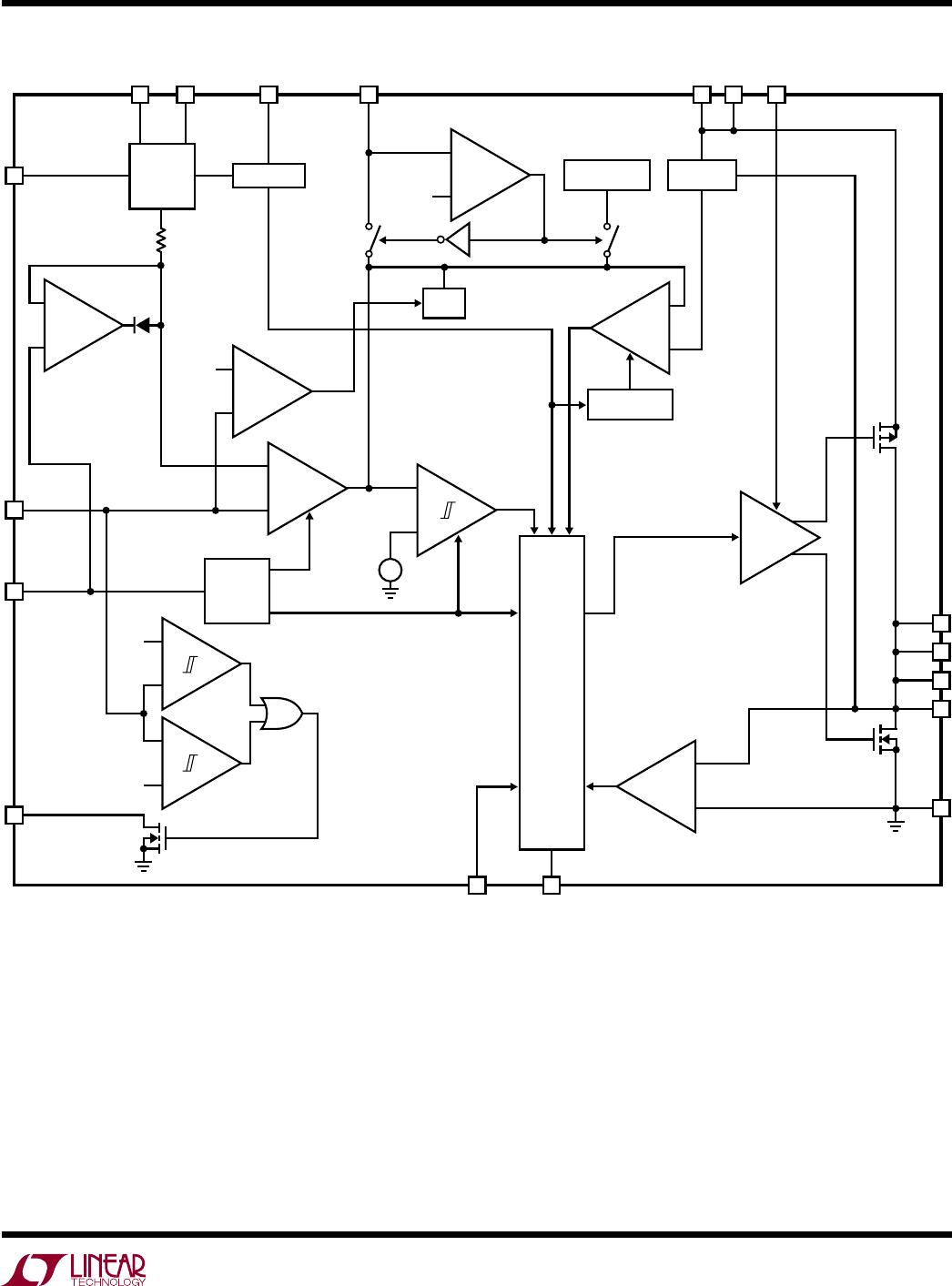
pin FuncTions
(QFN/FE)
DDR (Pin 1/Pin 8): DDR Mode Pin. Tying the DDR pin to
SV
IN
selects DDR mode and TRACK/SS can be used as
an external reference input. If DDR is tied to SGND, the
internal 0.6V reference will be used.
RT/SYNC (Pin 2/Pin 9): Oscillator Frequency. This pin
provides three ways of setting the constant switching
frequency:
1. Connecting a resistor from RT/SYNC to ground will set
the switching frequency based on the resistor value.
2. Driving the RT/SYNC pin with an external clock signal
will synchronize the LTC3612 to the applied frequency.
The slope compensation is automatically adapted to the
external clock frequency.
3. Tying the RT/SYNC pin to SV
IN
enables the internal
2.25MHz oscillator frequency.
SGND (Pin 3/Pin 10): Signal Ground. All small-signal and
compensation components should connect to this ground,
which in turn should connect to PGND at a single point.
NC (Pins 4, 7, 10/Pins 11, 13, 18): Can be connected to
ground or left open.
SW (Pins 5, 6, 11, 12/Pins 12, 14, 17, 19): Switch Node.
Connection to the inductor. This pin connects to the drains
of the internal synchronous power MOSFET switches.
PV
IN
(Pins 8, 9/Pins 15, 16): Power Input Supply. PV
IN
connects to the source of the internal P-channel power
MOSFET. This pin is independent of SV
IN
and may be con-
nected to the same voltage or to a lower voltage supply.
PV
IN_DRV
(Pin 13/Pin 20): Internal Gate Driver Input Sup-
ply. This pin must be connected to PV
IN
.
SV
IN
(Pin 14/Pin 1): Signal Input Supply. This pin pow-
ers the internal control circuitry and is monitored by the
undervoltage lockout comparator
.
RUN (Pin 15/Pin 2): Enable Pin. Forcing this pin to ground
shuts down the LTC3612. In shutdown, all functions are
disabled and the chip draws <1µA of supply current.
PGOOD (Pin 16/Pin 3): Power Good. This open-drain
output is pulled down to SGND on start-up and while the
FB voltage is outside the power good voltage window. If
the FB voltage increases and stays inside the power good
window for more than 105µs the PGOOD pin is released.
If the FB voltage leaves the power good window for more
than 105µs the PGOOD pin is pulled down.
In DDR mode (DDR = V
IN
), the power good window moves
in relation to the actual TRACK/SS pin voltage. During
up/down tracking the PGOOD pin is always pulled down.
In shutdown the PGOOD output will actively pull down
and may be used to discharge the output capacitors via
an external resistor.
MODE (Pin 17/Pin 4): Mode Selection. Tying the MODE
pin to SV
IN
or SGND enables pulse-skipping mode or Burst
Mode operation (with an internal Burst Mode clamp),
respectively. If this pin is held at slightly higher than half
of SV
IN
, forced continuous mode is selected. Connecting
this pin to an external voltage selects Burst Mode opera-
tion with the burst clamp set to the pin voltage. See the
Operation section for more details.
V
FB
(Pin 18/Pin 5): Voltage Feedback Input Pin. Senses
the feedback voltage from the external resistive divider
across the output.
ITH (Pin 19/Pin 6): Error Amplifier Compensation. The
current comparator’s threshold increases with this control
voltage. Tying this pin to SV
IN
enables internal compensa-
tion and AVP mode.
TRACK/SS (Pin 20/Pin 7): Track/External Soft-Start/
External Reference. Start-up behavior is programmable
with the TRACK/SS pin:
1. Tying this pin to SV
IN
selects the internal soft-start
circuit.
2. External soft-start timing can be programmed with a
capacitor to ground and a resistor to SV
IN
.
3. TRACK/SS can be used to force the LTC3612 to track
the start-up behavior of another supply.
The pin can also be used as external reference input. See
the Applications Information section for more information.
PGND (Pin 21/Pin 21): Power Ground. The exposed pad
connects to the source of the internal N-channel power
MOSFET. This pin should be connected close to the (–)
terminal of C
IN
and C
OUT
and soldered to PCB ground for
rated thermal performance.