LTC3612
13
3612fc
For more information www.linear.com/LTC3612
operaTion
Burst Mode Operation—External Clamp
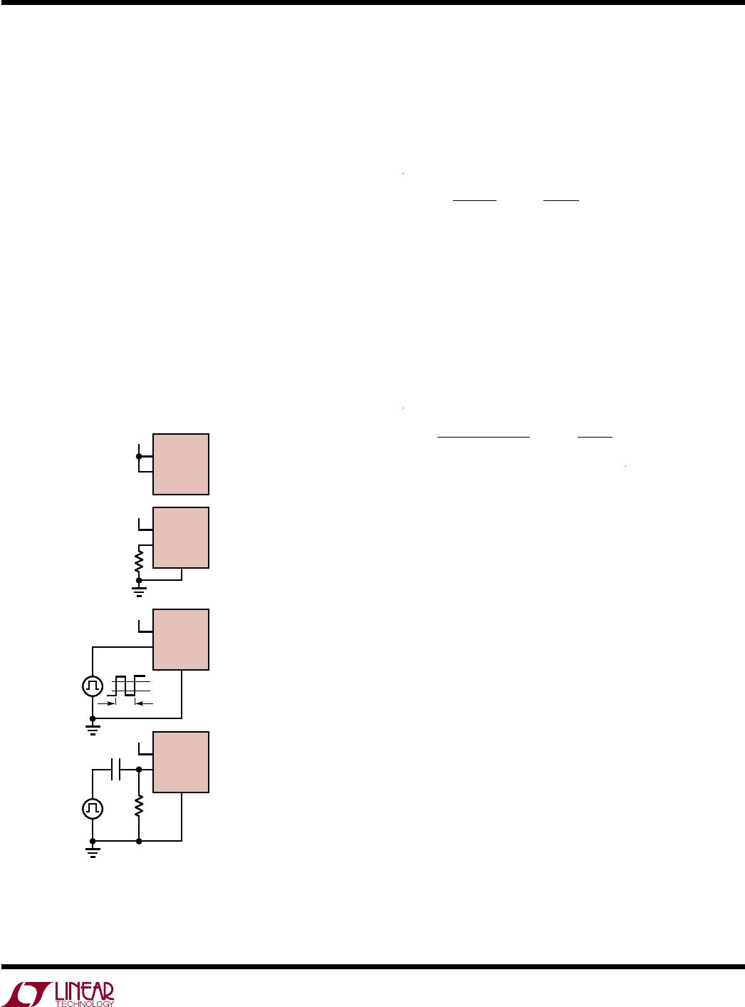
Connecting the MODE pin to a voltage in the range of 0.45V
to 0.8V enables Burst Mode operation with external clamp.
During this mode of operation the minimum voltage on
the ITH pin is externally set by the voltage on the MODE
pin. It is recommended to use Burst Mode operation with
an internal clamp for temperatures above 85°C ambient.
Pulse-Skipping Mode Operation
Pulse-skipping mode is similar to Burst Mode operation,
but the LTC3612 does not disable power to the internal
circuitry during sleep mode. This improves output voltage
ripple but uses more quiescent current, compromising
light load efficiency.
Tying the MODE pin to SV
IN
enables pulse-skipping mode.
As the load current decreases, the peak inductor current
will be determined by the voltage on the ITH pin until the
ITH voltage drops below the voltage level corresponding to
0A. At this point, the peak inductor current is determined
by the minimum on-time of the current comparator. If the
load demand is less than the average of the minimum on-
time inductor current, switching cycles will be skipped to
keep the output voltage in regulation.
Forced Continuous Mode
In forced continuous mode the inductor current is con
-
stantly cycled which creates a minimum output voltage
ripple at all output current levels.
Connecting the MODE pin to a voltage in the range of
1.1V to SV
IN
0.58 will enable forced continuous mode
operation.
At light loads, forced continuous mode operation is less
efficient than Burst Mode or pulse-skipping operation, but
may be desirable in some applications where it is neces
-
sary to keep switching harmonics out of the signal band.
For
ced continuous mode must be used if the output is
required to sink current.
Dropout Operation
As the input supply voltage
approaches the output voltage,
the duty cycle increases toward the maximum on-time.
Further reduction of the supply voltage forces the main
switch to remain on for more than one cycle, eventually
reaching 100% duty cycle. The output voltage will then be
determined by the input voltage minus the voltage drop
across the internal P-channel MOSFET and the inductor.
Low Supply Operation
The LTC3612 is designed to operate down to an input
supply voltage of 2.25V. An important consideration at low
input supply voltages is that the R
DS(ON)
of the P-channel
and N-channel power switches increases. The user should
calculate the power dissipation when the LTC3612 is used
at 100% duty cycle with low input voltages to ensure that
thermal limits are not exceeded. See the Typical Perfor
-
mance Characteristics graphs.
Short-Circuit Protection
The peak inductor current at which the current comparator
shuts off the top power switch is controlled by the voltage
on the ITH pin.
If the output current increases, the error amplifier raises the
ITH pin voltage until the average inductor current matches
the new load current. In normal operation the L
TC3612
clamps the maximum ITH pin voltage at approximately
1.05V which corresponds typically to 6A peak inductor
current.
When the output is shorted to ground, the inductor current
decays very slowly during a single switching cycle. The
LTC3612 uses two techniques to prevent current runaway
from occurring.
LTC3612
14
3612fc
For more information www.linear.com/LTC3612
applicaTions inForMaTion
If the output voltage drops below 50% of its nominal value,
the clamp voltage at ITH pin is lowered causing the maxi-
mum peak inductor current to decrease gradually with the
output voltage. When the output voltage reaches 0V the
clamp voltage at the ITH pin drops to 40% of the clamp
voltage during normal operation. The short-cir
cuit peak
inductor current is determined by the minimum on-time
of the L
TC3612, the input voltage and the inductor value.
This foldback behavior helps in limiting the peak inductor
current when the output is shorted to ground. It is disabled
during internal or external soft-start and tracking up/down
operation (see the Applications Information section).
A secondary limit is also imposed on the valley inductor
current. If the inductor current measured through the
bottom MOSFET increases beyond 6A typical, the top
power MOSFET will be held off and switching cycles will
be skipped until the inductor current is reduced.
operaTion
The basic LTC3612 application circuit is shown in Figure 1.
Operating Frequency
Selection of the operating frequency is a trade-off between
efficiency and component size. High frequency operation
allows the use of smaller inductor and capacitor values.
Operation at lower frequencies improves efficiency by
reducing internal gate charge losses but requires larger
inductance values and/or capacitance to maintain low
output ripple voltage.
The operating frequency of the LTC3612 is determined
by an external resistor that is connected between the RT/
SYNC pin and ground. The value of the resistor sets the
RUN
TRACK/SS
RT/SYNC
PGOOD
ITH
SGND
PGND
V
IN
2.25V TO 5.5V
PV
IN_DRV
DDR
SV
IN
LTC3612 SW
PV
IN
C
IN1
22µF
C
C
470pF
C
SS
22nF
L1
470nH
R1
392k
R2
196k
3612 F01
C
IN2
22µF
MODE V
FB
C
OUT1
47µF
C
OUT2
22µF
V
OUT
1.8V
3A
R
C
15k
R
T
130k
R
SS
2M
C
C1
10pF
(OPT)
Figure 1. 1.8V, 3A Step-Down Regulator
ramp current that is used to charge and discharge an
internal timing capacitor within the oscillator and can be
calculated by using the following equation:
R
T
=
3.8210
11
Hz
f
OSC
Hz
( )
16k
Although frequencies as high as 4MHz are possible, the
minimum on-time of the LTC3612 imposes a minimum
limit on the operating duty cycle. The minimum on-time
is typically 60ns; therefore, the minimum duty cycle is
equal to 100 • 60ns • f
OSC
(Hz)%.
Tying the RT/SYNC pin to SV
IN
sets the default internal
operating frequency to 2.25MHz ±20%.
LTC3612
15
3612fc
For more information www.linear.com/LTC3612
applicaTions inForMaTion
Frequency Synchronization
The LTC3612’s internal oscillator can be synchronized to
an external frequency by applying a square wave clock
signal to the RT/SYNC pin. During synchronization, the top
switch turn-on is locked to the falling edge of the external
frequency source. The synchronization frequency range
is 300kHz to 4MHz. During synchronization all operation
modes can be selected.
It is recommended that the regulator is powered down
(RUN pin to ground) before removing the clock signal on
the RT/SYNC pin in order to reduce inductor current ripple.
AC coupling should be used if the external clock generator
cannot provide a continuous clock signal throughout start-
up, operation and shutdown of the LTC3612. The size of
capacitor C
SYNC
depends on parasitic capacitance on the
RT/SYNC pin and is typically in the range of 10pF to 22pF
Inductor Selection
For a given input and output voltage, the inductor value
and operating frequency determine the ripple current. The
ripple current I
L
increases with higher V
IN
and decreases
with higher inductance:
I
L
=
V
OUT
f
SW
L
1–
V
OUT
V
IN
Having a lower ripple current reduces the core losses
in the inductor, the ESR losses in the output capacitors
and the output voltage ripple. A reasonable starting point
for selecting the ripple current is I
L
= 0.3 I
OUT(MAX)
.
The largest ripple current occurs at the highest V
IN
. To
guarantee that the ripple current stays below a specified
maximum, the inductor value should be chosen according
to the following equation:
L =
V
OUT
f
SW
I
L(MAX)
1–
V
OUT
V
IN
The inductor value will also have an effect on Burst Mode
operation. The transition to low current operation begins
when the peak inductor current falls below a level set by the
burst clamp. Lower inductor values result in higher ripple
current which causes this to occur at lower load currents.
This causes a dip in efficiency in the upper range of low
current operation. In Burst Mode operation, lower induc
-
tance values will cause the burst frequency to increase.
Inductor Core
Selection
Once the value for L is known, the type of inductor must be
selected. Actual core loss is independent of core size for
fixed inductor value, but it is very dependent on the induc
-
tance selected. As the inductance increases, core losses de-
crease. Unfortunately, increased inductance requires more
turns of wire and therefore, copper losses will increase.
Ferrite designs have ver
y low core losses and are pre
-
ferred at high switching frequencies, so design goals
can concentrate on copper loss and preventing satura-
tion. Ferrite core material saturates “hard,” meaning
that
inductance collapses abruptly
when the peak design
current is exceeded. This results in an abrupt increase in
LTC3612
SV
IN
V
IN
RT/SYNC
LTC3612
SV
IN
V
IN
0.4V
RT/SYNC
R
T
R
T
SGND
LTC3612
SV
IN
f
OSC
2.25MHz
f
OSC
1/T
P
f
OSC
1/R
T
V
IN
RT/SYNC
SGND
T
P
1.2V
0.3V
LTC3612
SV
IN
f
OSC
1/T
P
V
IN
C
SYNC
RT/SYNC
SGND
3612 F02
Figure 2. Setting the Switching Frequency

LTC3612EUDC#PBF

Mfr. #:
Manufacturer:
Analog Devices / Linear Technology
Description:
Switching Voltage Regulators 3A, 4MHz, Monolithic Synchronous Step-Down Regulator
Lifecycle:
New from this manufacturer.
Delivery:
DHL FedEx Ups TNT EMS
Payment:
T/T Paypal Visa MoneyGram Western Union