LTC3612
16
3612fc
For more information www.linear.com/LTC3612
applicaTions inForMaTion
inductor ripple current and consequently output voltage
ripple. Do not allow a ferrite core to saturate and select
external inductors respecting the temperature range of
the application!
Different core materials and shapes will change the size/
current and price/current relationship of an inductor. Toroid
or shielded pot cores in ferrite or permalloy materials are
small and do not radiate much energy, but generally cost
more than powdered iron core inductors with similar
characteristics. The choice of which style inductor to use
mainly depends on the price versus size requirements
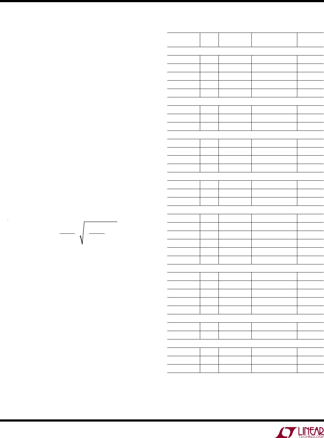
and any radiated field/EMI requirements. Table 1 shows
some typical surface mount inductors that work well in
LTC3612 applications.
Input Capacitor (C
IN
) Selection
In continuous mode, the source current of the top P-
channel MOSFET is a square wave of duty cycle V
OUT
/V
IN
.
To prevent large voltage transients, a low ESR capacitor
sized for the maximum RMS current must be used at V
IN
.
The maximum RMS capacitor current is given by:
I
RMS
=I
OUT(MAX)
V
OUT
V
IN
V
IN
V
OUT
1
This formula has a maximum at V
IN
= 2V
OUT
, where I
RMS
=
I
OUT
/2. This simple worst-case condition is commonly used
for design because even significant deviations do not offer
much relief. Note that ripple current ratings from capacitor
manufacturers are often based on only 2000 hours of life
which makes it advisable to further derate the capacitor,
or choose a capacitor rated at a higher temperature than
required. Generally select the capacitors respecting the
temperature range of the application! Several capacitors
may also be paralleled to meet size or height requirements
in the design.
Output Capacitor (C
OUT
) Selection
The selection of C
OUT
is typically driven by the required
ESR to minimize voltage ripple and load step transients
(low ESR ceramic capacitors are discussed in the next
section). Typically, once the ESR requirement is satisfied,
Table 1. Representative Surface Mount Inductors
INDUCTANCE
(µH)
DCR
(mΩ)
MAX
CURRENT (A)
DIMENSIONS
(mm)
HEIGHT
(mm)
Vishay IHLP-2525AH-01 Series
0.33 7 12 6.7 × 7 1.8
0.47 9 11 6.7 × 7 1.8
0.68 13 9 6.7 × 7 1.8
0.82 15 8 6.7 × 7 1.8
1.0 18 7 6.7 × 7 1.8
Vishay IHLP-1616BZ-01 Series
0.22 8 24 4.3 × 4.7 2
0.47 18 11.5 4.3 × 4.7 2
1.00 37 8.5 4.3 × 4.7 2
Sumida CDMC6D28 Series
0.3 3.2 15.4 6.7 × 7.25 3
0.47 4.2 13.6 6.7 × 7.25 3
0.68 5.4 11.3 6.7 × 7.25 3
1 8.8 8.8 6.7 × 7.25 3
NEC/Tokin MPLC0730L Series
0.47
4.5 16.6 6.9 × 7.7 3.0
0.75 7.5 12.2 6.9 × 7.7 3.0
1.0 9.0 10.6 6.9 × 7.7 3.0
Cooper HCP0703 Series
0.22 2.8 23 7 × 7.3 3.0
0.47 4.2 17 7 × 7.3 3.0
0.68 5.5 15 7 × 7.3 3.0
0.82 8.0 13 7 × 7.3 3.0
1.0 10.0 11 7 × 7.3 3.0
1.5 9.6 61 6.9 × 7.3 3.2
Würth Elektronik WE-HC744312 Series
0.25 2.5 18 7 × 7.7 3.8
0.47 3.4 16 7 × 7.7 3.8
0.72 7.5 12 7 × 7.7 3.8
1.0 9.5 11 7 × 7.7 3.8
1.5 10.5 9 7 × 7.7 3.8
Coilcraft DO1813H Series
0.33 4 10 8.9 × 6.1 5
0.56 10 7.7 8.9 × 6.1 5
Coilcraft v Series
0.27 0.1 14 7.5 × 6.7 3
0.35 0.1 11 7.5 × 6.7 3
0.4 0.1 8 7.5 × 6.7 3
LTC3612
17
3612fc
For more information www.linear.com/LTC3612
applicaTions inForMaTion
the capacitance is adequate for filtering. The output ripple
V
OUT
is determined by:
V
OUT
I
L
ESR+
1
8 f
SW
C
OUT
where f
OSC
= operating frequency, C
OUT
= output capaci-
tance and I
L
= ripple current in the inductor. The output
ripple is highest at maximum input voltage since I
L
increases with input voltage.
In surface mount applications, multiple capacitors may
have to be paralleled to meet the capacitance, ESR or RMS
current handling requirement of the application. Aluminum
electrolytic, special polymer, ceramic and dry tantalum
capacitors are all available in surface mount packages.
Tantalum capacitors have the highest capacitance density,
but can have higher ESR and must be surge tested for
use in switching power supplies. Aluminum electrolytic
capacitors have significantly higher ESR, but can often
be used in extremely cost-sensitive applications provided
that consideration is given to ripple current ratings and
long term reliability.
Ceramic Input and Output Capacitors
Ceramic capacitors have the lowest ESR and can be cost
effective, but also have the lowest capacitance density,
high voltage and temperature coefficients, and exhibit
audible piezoelectric effects. In addition, the high-Q of
ceramic capacitors along with trace inductance can lead
to significant ringing.
They are attractive for switching regulator use because
of their very low ESR, but great care must be taken when
using only ceramic input and output capacitors.
Ceramic capacitors are prone to temperature effects
which require the designer to check loop stability over
the operating temperature range. To minimize their large
temperature and voltage coefficients, only X5R or X7R
ceramic capacitors should be used.
When a ceramic capacitor is used at the input and the power
is being supplied through long wires, such as from a wall
adapter, a load step at the output can induce ringing at the
V
IN
pin. At best, this ringing can couple to the output and
be mistaken as loop instability. At worst, the ringing at the
input can be large enough to damage the part.
Since the ESR of a ceramic capacitor is so low, the input
and output capacitor must instead fulfill a charge storage
requirement. During a load step, the output capacitor must
instantaneously supply the current to support the load until
the feedback loop raises the switch current enough to sup
-
port the load. The time required for the feedback loop to
respond is dependent on the compensation components
and the output capacitor size. T
ypically
, 3 to 4 cycles are
required to respond to a load step, but only in the first cycle
does the output drop linearly. The output droop, V
DROOP
,
is usually about 2 to 4 times the linear drop of the first
cycle; however, this behavior can vary depending on the
compensation component values. Thus, a good place to
start is with the output capacitor size of approximately:
C
OUT
3.5 I
OUT
f
SW
V
DROOP
This is only an approximation; more capacitance may
be needed depending on the duty cycle and load step
requirements.
In most applications, the input capacitor is merely required
to supply high frequency bypassing, since the impedance
to the supply is very low.
Output Voltage Programming
The output voltage is set by an external resistive divider
according to the following equation:
V
OUT
= 0.6 1+
R1
R2
V
The resistive divider allows pin V
FB
to sense a fraction of
the output voltage, as shown in Figure 1.
LTC3612
18
3612fc
For more information www.linear.com/LTC3612
Burst Clamp Programming
If the voltage on the MODE pin is less than 0.8V, Burst
Mode operation is enabled.
If the voltage on the MODE pin is less than 0.3V, the in
-
ternal default burst clamp level is selected. The minimum
voltage on the ITH pin is typically 525mV (internal clamp).
If the voltage is between 0.45V and 0.8V, the voltage on
the MODE pin (V
BURST
) is equal to the minimum voltage
on the ITH pin (external clamp) and determines the burst
clamp level I
BURST
(typically from 0A to 3.5A).
When the ITH voltage falls below the internal (or external)
clamp voltage, the sleep state is enabled.
As the output load current drops, the peak inductor current
decreases to keep the output voltage in regulation. When
the output load current demands a peak inductor current
that is less than I
BURST
, the burst clamp will force the peak
inductor current to remain equal to I
BURST
regardless of
further reductions in the load current.
Since the average inductor current is greater than the out
-
put load current, the voltage on the ITH pin will decrease.
When the ITH voltage drops, sleep mode is enabled in
which both power switches are shut off along with most
of the circuitry to minimize power consumption. All cir
-
cuitry is turned back on and the power switches resume
operation when the output voltage drops out of regulation.
The value for I
BURST
is determined by the desired amount
of output voltage ripple. As the value of I
BURST
increases,
the sleep period between pulses and the output voltage
ripple increase. Note that for very high V
BURST
voltage
settings, the power good comparator may trip, since the
output ripple may get bigger than the power good window.
Pulse-skipping mode, which is a compromise between low
output voltage ripple and efficiency, can be implemented
by connecting MODE to SV
IN
. This sets I
BURST
to 0A. In
this condition, the peak inductor current is limited by the
minimum on-time of the current comparator. The lowest
output voltage ripple is achieved while still operating
discontinuously. During very light output loads, pulse
skipping allows only a few switching cycles to skip while
maintaining the output voltage in regulation.
Internal and External Compensation
The regulator loop response can be checked by looking at
the load current transient response. Switching regulators
take several cycles to respond to a step in DC load current.
When a load step occurs, V
OUT
shifts by an amount equal
to I
LOAD(ESR)
, where ESR is the effective series resistance
of C
OUT
. I
LOAD
also begins to charge or discharge C
OUT
,
generating the feedback error signal that forces the regula-
tor to adapt to the current change and return V
OUT
to its
steady-state value. During this recovery time V
OUT
can
be monitored for excessive overshoot or ringing, which
would indicate a stability problem. The availability of the
ITH pin allows the transient response to be optimized over
a wide range of output capacitance.
The ITH external components (R
C
and C
C
) shown in Fig-
ure
1 provide adequate compensation as a starting point
for most applications. The values can be modified slightly
to optimize transient response once the final PCB layout
is done and the particular output capacitor type and value
have been determined. The output capacitors need to be
selected because the various types and values determine
the loop gain and phase. The gain of the loop will be in
-
creased by increasing R
C
and the bandwidth of the loop
will be increased by decreasing C
C
. If R
C
is increased by
the same factor that C
C
is decreased, the zero frequency
will be kept the same, thereby keeping the phase shift the
same in the most critical frequency range of the feedback
loop. The output voltage settling behavior is related to the
stability of the closed-loop system. The external capaci
-
tor, C
C1
, (Figure 1) is not needed for loop stability, but it
helps filter out any high frequency noise that may couple
onto that node. The general purpose buck regulator ap
-
plication in the Typical Applications section uses a faster
compensation to improve load step response.
A second, more severe transient is caused by switching
in loads with large (>1μF) supply bypass capacitors. The
discharged bypass capacitors are effectively put in parallel
with C
OUT
, causing a rapid drop in V
OUT
. No regulator can
alter its delivery of current quickly enough to prevent this
sudden step change in output voltage if the load switch
resistance is low and it is driven quickly. More output
capacitance may be required depending on the duty cycle
and load step requirements.
applicaTions inForMaTion

LTC3612EUDC#PBF

Mfr. #:
Manufacturer:
Analog Devices / Linear Technology
Description:
Switching Voltage Regulators 3A, 4MHz, Monolithic Synchronous Step-Down Regulator
Lifecycle:
New from this manufacturer.
Delivery:
DHL FedEx Ups TNT EMS
Payment:
T/T Paypal Visa MoneyGram Western Union