LTC3612
4
3612fc
For more information www.linear.com/LTC3612
Note 1: Stresses beyond those listed under Absolute Maximum Ratings
may cause permanent damage to the device. Exposure to any Absolute
Maximum Rating condition for extended periods may affect device
reliability and lifetime.
Note 2: The LTC3612 is tested under pulsed load conditions such that
T
J
T
A
. The LTC3612E is guaranteed to meet performance specifications
from 0°C to 85°C junction temperature. Specifications over the
–40°C to 125°C operating junction temperature range are assured by
design, characterization and correlation with statistical process controls.
The LTC3612I is guaranteed over the full –40°C to 125°C operating
junction temperature range. The LTC3612H is guaranteed to meet
specifications over the –40°C to 150°C operating temperature range. The
LTC3612MP is guaranteed and tested to meet specifications over the full
–55°C to 150°C operating temperature range. Note that the maximum
ambient temperature consistent with these specifications is determined by
specific operating conditions in conjunction with board layout, the rated
package thermal impedance and other environmental factors. The junction
temperature
(T
J
, in °C) is calculated from the ambient temperature (T
A
, in °C) and
power dissipation (P
D
, in watts) according to the formula:
T
J
= T
A
+ (P
D
θ
JA
),
where θ
JA
(in °C/W) is the package thermal impedance.
elecTrical characTerisTics
The l denotes the specifications which apply over the specified operating
junction temperature range, otherwise specifications are at T
A
= 25°C (Note 2). V
IN
= 3.3V, RT/SYNC = SV
IN
, unless otherwise specified.
SYMBOL PARAMETER CONDITIONS MIN TYP MAX UNITS
PGOOD Power Good Voltage Windows TRACK/SS = SV
IN
, Entering Window
V
FB
Ramping Up
V
FB
Ramping Down
–3.5
3.5
–6
6
%
%
TRACK/SS = SV
IN
, Leaving Window
V
FB
Ramping Up
V
FB
Ramping Down
9
–9
11
–11
%
%
t
PGOOD
Power Good Blanking Time Entering and Leaving Window 70 105 140 µs
R
PGOOD
Power Good Pull-Down On-Resistance 8 17 33 Ω
V
RUN
RUN Voltage Input High
Input Low
l
l
1
0.4
V
V
Note 3: This parameter is tested in a feedback loop which ser
vos V
FB
to
the midpoint for the error amplifier (V
ITH
= 0.75V).
Note 4: External compensation on ITH pin.
Note 5: Tying the ITH pin to SV
IN
enables the internal compensation and
AVP mode.
Note 6: Dynamic supply current is higher due to the internal gate charge
being delivered at the switching frequency.
Note 7: See description of the TRACK/SS pin in the Pin Functions section.
Note 8: In sourcing mode the average output current is flowing out of SW
pin. In sinking mode the average output current is flowing into the SW Pin.
Note 9: See description of the MODE pin in the Pin Functions section.
Note 10: Guaranteed by correlation and design to wafer level
measurements for QFN packages.
Note 11: This IC includes overtemperature protection that is intended
to protect the device during momentary overload conditions. Junction
temperature will exceed 150°C when overtemperature protection is active.
Continuous operation above the specified maximum operating junction
temperature may impair device reliability.
LTC3612
5
3612fc
For more information www.linear.com/LTC3612
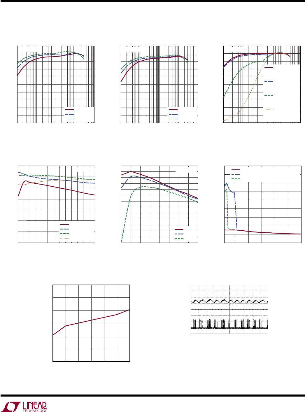
Typical perForMance characTerisTics
Efficiency vs Load Current
(V
MODE
= 0V)
Efficiency vs Load Current
(V
MODE
= 0V)
Efficiency vs Load Current
Efficiency vs Input Voltage
(V
MODE
= 0V)
Efficiency vs Frequency
(V
MODE
= 0V), I
OUT
= 1A
Load Regulation
Line Regulation Burst Mode Operation
OUTPUT CURRENT (mA)
30
EFFICIENCY (%)
90
100
20
10
80
50
70
60
40
1 100 1000 10000
3612 G01
0
10
V
IN
= 5V
V
IN
= 3.3V
V
IN
= 2.5V
V
OUT
= 1.8V
OUTPUT CURRENT (mA)
30
EFFICIENCY (%)
90
100
20
10
80
50
70
60
40
1 100 1000 10000
3612 G02
0
10
V
IN
= 5V
V
IN
= 3.3V
V
IN
= 2.5V
V
OUT
= 1.2V
OUTPUT CURRENT (mA)
30
EFFICIENCY (%)
90
100
20
10
80
50
70
60
40
1 100 1000 10000
3612 G03
0
10
Burst Mode
EXTERNAL
CLAMP = 0.7V
Burst Mode
INTERNAL
CLAMP
PULSE-
SKIPPING
MODE
FORCED
CONTINUOUS
MODE
V
OUT
= 1.8V
INPUT VOLTAGE (V)
2.25
30
EFFICIENCY (%)
40
60
70
80
100
3612 G04
50
90
3.75
3.25
5.25
2.75
4.25 4.75
I
OUT
= 3mA
I
OUT
= 300mA
I
OUT
= 1A
I
OUT
= 3A
V
OUT
= 1.8V
FREQUENCY (MHz)
0.5
82
EFFICIENCY (%)
83
84
85
86
95
89
91
93
94
92
88
90
1.0
1.5 2.0 3.02.5 3.5
3612 G05
4.0 4.5
87
1µH
0.68µH
0.33µH
V
OUT
= 1.8V
OUTPUT CURRENT (mA)
0
–0.3
V
OUT
ERROR (%)
–0.1
0.3
0.5
0.7
2000
1.5
3612 G06
0.1
1000
500
2500
1500 3000
0.9
1.1
1.3
FORCED CONTINUOUS MODE
INTERNAL Burst Mode OPERATION
PULSE-SKIPPING MODE
V
OUT
= 1.8V
INPUT VOLTAGE (V)
2.20
–0.3
V
OUT
ERROR (%)
–0.2
–0.1
0
0.1
0.3
2.75
3.30 3.85 4.40
3612 G07
4.95 5.50
0.2
V
OUT
20mV/DIV
I
L
500mA/DIV
20µs/DIV
3612 G08
V
OUT
= 1.8V
I
OUT
= 75mA
V
MODE
= 0V
V
IN
= 3.3V, RT/SYNC = SV
IN
, unless otherwise noted.
LTC3612
6
3612fc
For more information www.linear.com/LTC3612
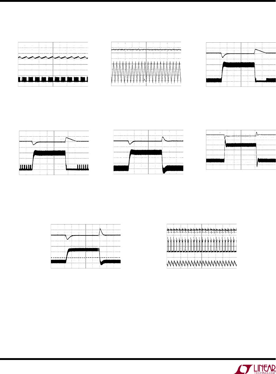
Sinking Current
Load Step Transient in Forced
Continuous Mode without AVP Mode
Load Step Transient in Forced
Continuous Mode with AVP Mode
Load Step Transient in Forced
Continuous Mode Sourcing and
Sinking Current
V
OUT
200mV/DIV
I
L
1A/DIV
50µs/DIV
3612 G13
V
OUT
= 1.8V
I
LOAD
= 100mA TO 3A
V
MODE
= 1.5V
COMPENSATION FIGURE 1
V
OUT
100mV/DIV
I
L
1A/DIV
50µs/DIV
3612 G14
V
OUT
= 1.8V
I
LOAD
= 100mA TO 3A
V
MODE
= 1.5V
V
ITH
= V
IN
OUTPUT CAPACITOR VALUE FIGURE 1
V
OUT
200mV/DIV
I
L
2A/DIV
0A
50µs/DIV
3612 G15
V
OUT
= 1.8V
I
LOAD
= –1.5A TO 3A
V
MODE
= 1.5V
COMPENSATION FIGURE 1
V
OUT
20mV/DIV
SW
2V/DIV
I
L
500mA/DIV
1µs/DIV
3612 G16
V
OUT
= 1.2V
I
OUT
= –1A
V
MODE
= 1.5V
Typical perForMance characTerisTics
V
IN
= 3.3V, RT/SYNC = SV
IN
, unless otherwise noted.
Load Step Transient in
Pulse-Skipping Mode
Load Step Transient in
Burst Mode Operation
V
OUT
200mV/DIV
I
L
1A/DIV
50µs/DIV
3612 G11
V
OUT
= 1.8V
I
LOAD
= 100mA TO 3A
V
MODE
= 3.3V
COMPENSATION FIGURE 1
V
OUT
200mV/DIV
I
L
1A/DIV
50µs/DIV
3612 G12
V
OUT
= 1.8V
I
LOAD
= 100mA TO 3A
V
MODE
= 0V
COMPENSATION FIGURE 1
Pulse-Skipping Mode Operation
Forced Continuous Mode Operation
V
OUT
20mV/DIV
I
L
500mA/DIV
20µs/DIV
3612 G09
V
OUT
= 1.8V
I
OUT
= 75mA
V
MODE
= 3.3V
V
OUT
20mV/DIV
I
L
200mA/DIV
1µs/DIV
3612 G10
V
OUT
= 1.8V
I
OUT
= 100mA
V
MODE
= 1.5V

LTC3612EUDC#PBF

Mfr. #:
Manufacturer:
Analog Devices / Linear Technology
Description:
Switching Voltage Regulators 3A, 4MHz, Monolithic Synchronous Step-Down Regulator
Lifecycle:
New from this manufacturer.
Delivery:
DHL FedEx Ups TNT EMS
Payment:
T/T Paypal Visa MoneyGram Western Union