DRAM Package Electrical Specifications
Table 6: DRAM Package Electrical Specifications for x16 Devices
Notes 1–4 apply to the entire table
Parameter Symbol
DDR4-1600, -1866 DDR4-2133, -2400 DDR4-2666, -2933
Unit NotesMin Max Min Max Min Max
Input/
output
Zpkg Z
IO
30 50 30 50 30 50 ohm 5, 6
Package delay Td
IO
60 120 60 120 60 120 ps 6 , 7
Lpkg L
IO
5.0 5.0 5.0 nH
Cpkg C
IO
3.0 3.0 3.0 pF
DQSL_t/
DQSL_c/
DQSU_t/
DQSU_c
Zpkg Z
IO DQS
30 50 30 50 30 50 ohm 5
Package delay Td
IO DQS
60 120 60 120 60 120 ps 7
Lpkg L
IO DQS
5.0 5.0 5.0 nH
Cpkg C
IO DQS
3.0 3.0 3.0 pF
DQSL_t/
DQSL_c,
DQSU_t/
DQSU_c,
Delta Zpkg DZ
IO DQS
20 20 20 ohm 5, 8
Delta delay DTd
IO DQS
45 45 45 ps 7, 8
Input CTRL
pins
Zpkg Z
I CTRL
35 65 35 65 35 65 ohm 5, 9
Package delay Td
I CTRL
75 120 75 120 75 120 ps 7, 9
Lpkg L
I CTRL
6.5 6.5 6.5 nH
Cpkg C
I CTRL
2.5 2.5 2.5 pF
Input CMD
ADD pins
Zpkg Z
I ADD CMD
35 65 35 65 35 65 ohm 5, 10
Package delay Td
I ADD CMD
70 125 70 125 70 125 ps 7, 10
Lpkg L
I ADD CMD
6.5 6.5 6.5 nH
Cpkg C
I ADD CMD
3.0 3.0 3.0 pF
CK_t, CK_c Zpkg Z
CK
30 55 30 55 30 55 ohm 5
Package delay Td
CK
80 135 80 135 80 135 ps 7
Delta Zpkg DZ
DCK
0.5 0.5 0.5 ohm 5, 11
Delta delay DTd
DCK
1.2 1.2 1.2 ps 7, 11
Input CLK Lpkg L
I CLK
6.0 6.0 6.0 nH
Cpkg C
I CLK
3.0 3.0 3.0 pF
ZQ Zpkg Z
O ZQ
40 40 40 ohm 5
ZQ delay Td
O ZQ
30 135 30 135 30 135 ps 7
ALERT Zpkg Z
O ALERT
30 55 30 55 30 55 ohm 5
ALERT delay Td
O ALERT
65 110 65 110 65 110 ps 7
Notes:
1. The package parasitic (L and C) are not subject to production testing. If the package par-
asitic (L and C) are measured, the capacitance is measured with V
DD
, V
DDQ
, V
SS
, and V
SSQ
shorted with all other signal pins floating. The inductance is measured with V
DD
, V
DDQ
,
V
SS
, and V
SSQ
shorted and all other signal pins shorted at the die, not pin, side.
2. Package implementations should satisfy targets if the Zpkg and package delay fall with-
in the ranges shown, and the maximum Lpkg and Cpkg do not exceed the maximum
16Gb: x16 TwinDie Single Rank DDR4 SDRAM
DRAM Package Electrical Specifications
CCMTD-1725822587-9947
16gb_x16_1cs_TwinDie.pdf - Rev. G 06/18 EN
10
Micron Technology, Inc. reserves the right to change products or specifications without notice.
© 2015 Micron Technology, Inc. All rights reserved.
values shown. The package design targets are provided for reference, system signal sim-
ulations should not use these values but use the Micron package model.
3. It is assumed that Lpkg can be approximated as Lpkg = Z
O
× Td.
4. It is assumed that Cpkg can be approximated as Cpkg = Td/Z
O
.
5. Package-only impedance (Zpkg) is calculated based on the Lpkg and Cpkg total for a
given pin where: Zpkg (total per pin) = SQRT (Lpkg/Cpkg).
6. Z
IO
and Td
IO
apply to DQ, DM, DQS_c, DQS_t, TDQS_t, and TDQS_c.
7. Package-only delay (Tpkg) is calculated based on Lpkg and Cpkg total for a given pin
where: Tdpkg (total per pin) = SQRT (Lpkg × Cpkg).
8. Absolute value of ZIO (DQS_t), ZIO (DQS_c) for impedance (Z) or absolute value of TdIO
(DQS_t), TdIO (DQS_c) for delay (Td).
9. Z
I CTRL
and Td
I CTRL
apply to ODT, CS_n, and CKE.
10. Z
I ADD CMD
and Td
I ADD CMD
apply to A[17:0], BA[1:0], BG[1:0], RAS_n CAS_n, and WE_n.
11. Absolute value of ZCK_t, ZCK_c for impedance (Z) or absolute value of TdCK_t, TdCK_c
for delay (Td).
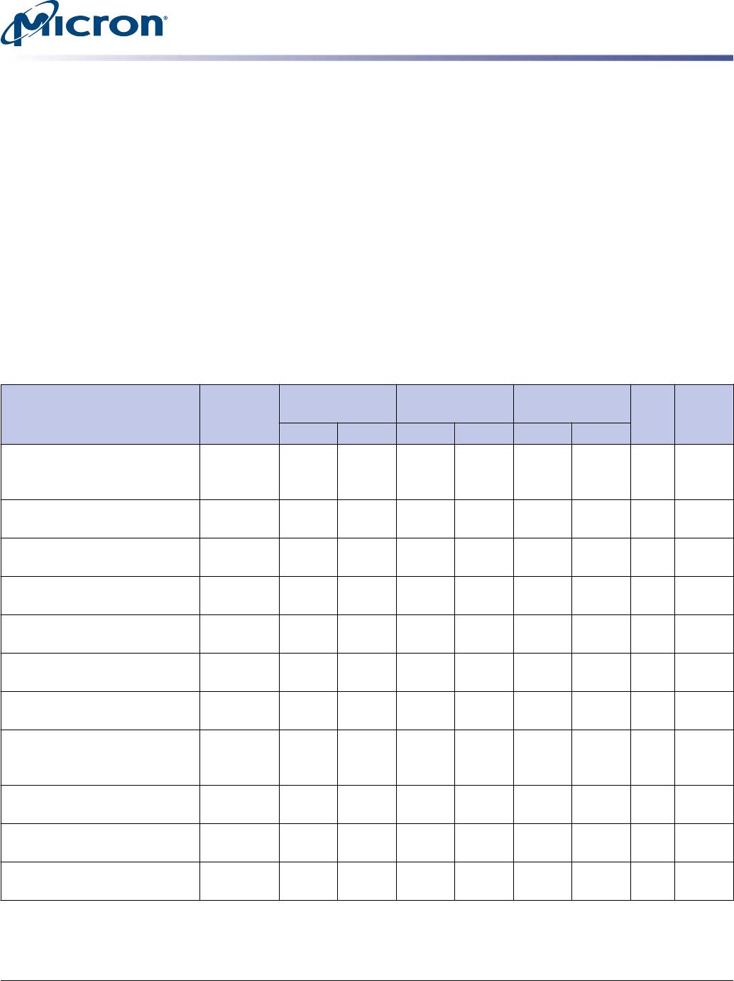
Table 7: Pad Input/Output Capacitance
Parameter Symbol
DDR4-1600,
-1866, -2133
DDR4-2400,
-2666 DDR4-2933
Unit NotesMin Max Min Max Min Max
Input/output capacitance: DQ,
DM, DQS_t, DQS_c, TDQS_t,
TDQS_c
C
IO
1.8 2.8 1.8 2.8 1.8 2.8 pF 1, 2, 3
Input capacitance: CK_t and
CK_c
C
CK
2.1 2.9 2.1 2.9 2.1 2.9 pF 1, 2, 3, 4
Input capacitance delta: CK_t
and CK_c
C
DCK
0 0.05 0 0.05 0 0.05 pF 1, 2, 3, 5
Input/output capacitance delta:
DQS_t and DQS_c
C
DDQS
0 0.05 0 0.05 0 0.05 pF 1, 3
Input capacitance: CTRL, ADD,
CMD input-only pins
C
I
1.6 2.6 1.6 2.6 1.6 2.6 pF 1, 3, 6
Input capacitance delta: All
CTRL input-only pins
C
DI_CTRL
–0 .9 0.9 –0 .9 0.9 –0 .9 0.9 pF 1, 3, 7
Input capacitance delta: All
ADD/CMD input-only pins
C
DI_ADD_CMD
–0 .9 0.9 –0 .9 0.9 –0 .9 0.9 pF 1, 3, 8, 9
Input/output capacitance delta:
DQ, DM, DQS_t, DQS_c, TDQS_t,
TDQS_c
C
DIO
–0.16 0.16 –0.16 0.16 –0.16 0.16 pF 1, 2, 10,
11
Input/output capacitance:
ALERT pin
C
ALERT
1.1 2.3 1.1 2.3 1.1 2.3 pF 1, 3
Input/output capacitance: ZQ
pin
C
ZQ
3.7 3.7 3.7 pF 1, 3, 12
Input/output capacitance: TEN
pin
C
TEN
0.2 2.3 0.2 2.3 0.2 2.3 pF 1, 3, 13
Notes:
1. Although the DM, TDQS_t, and TDQS_c pins have different functions, the loading
matches DQ and DQS.
16Gb: x16 TwinDie Single Rank DDR4 SDRAM
DRAM Package Electrical Specifications
CCMTD-1725822587-9947
16gb_x16_1cs_TwinDie.pdf - Rev. G 06/18 EN
11
Micron Technology, Inc. reserves the right to change products or specifications without notice.
© 2015 Micron Technology, Inc. All rights reserved.
2. This parameter is not subject to a production test; it is verified by design and characteri-
zation and are provided for reference; system signal simulations should not use these
values but use the Micron package model. The capacitance, if and when, is measured ac-
cording to the JEP147 specification, “Procedure for Measuring Input Capacitance Using
a Vector Network Analyzer (VNA),” with V
DD
, V
DDQ
, V
SS
, and V
SSQ
applied and all other
pins floating (except the pin under test, CKE, RESET_n and ODT, as necessary). V
DD
=
V
DDQ
= 1.5V, V
BIAS
= V
DD
/2 and on-die termination off.
3. This parameter applies to SR x16 TwinDie, obtained by de-embedding the package L and
C parasitics.
4. C
DIO
= C
IO
(DQ, DM) - 0.5 × (C
IO
(DQS_t) + C
IO
(DQS_c)).
5. Absolute value of C
IO
(DQS_t), C
IO
(DQS_c)
6. Absolute value of CCK_t, CCK_c
7. C
I
applies to ODT, CS_n, CKE, A[15:0], BA[1:0], RAS_n, CAS_n, and WE_n.
8. C
DI_CTRL
applies to ODT, CS_n, and CKE.
9. C
DI_CTRL
= C
I
(CTRL) - 0.5 × (C
I
(CLK_t) + C
I
(CLK_c)).
10. C
DI_ADD_CMD
applies to A[15:0], BA1:0], RAS_n, CAS_n and WE_n.
11. C
DI_ADD_CMD
= C
I
(ADD_CMD) - 0.5 × (C
I
(CLK_t) + C
I
(CLK_c)).
12. Maximum external load capacitance on ZQ pin: 5pF.
13. Only applicable if TEN pin does not have an internal pull-up.
16Gb: x16 TwinDie Single Rank DDR4 SDRAM
DRAM Package Electrical Specifications
CCMTD-1725822587-9947
16gb_x16_1cs_TwinDie.pdf - Rev. G 06/18 EN
12
Micron Technology, Inc. reserves the right to change products or specifications without notice.
© 2015 Micron Technology, Inc. All rights reserved.

MT40A1G16WBU-075E:B

Mfr. #:
Manufacturer:
Micron
Description:
IC DRAM 16G PARALLEL 1.33GHZ
Lifecycle:
New from this manufacturer.
Delivery:
DHL FedEx Ups TNT EMS
Payment:
T/T Paypal Visa MoneyGram Western Union